SGLS162I April 2003 – March 2016 TPS793-Q1
PRODUCTION DATA.
- 1 Features
- 2 Applications
- 3 Description
- 4 Revision History
- 5 Voltage Options
- 6 Pin Configuration and Functions
- 7 Specifications
- 8 Detailed Description
- 9 Application and Implementation
- 10Power Supply Recommendations
- 11Layout
- 12Device and Documentation Support
- 13Mechanical, Packaging, and Orderable Information
7 Specifications
7.1 Absolute Maximum Ratings
over operating free-air temperature range (unless otherwise noted)(1)| MIN | MAX | UNIT | |||
|---|---|---|---|---|---|
| Input voltage(2) | –0.3 | 6 | V | ||
| Voltage range at EN | –0.3 | VI + 0.3 | V | ||
| Voltage on OUT | –0.3 | 6 | V | ||
| Peak output current | Internally limited | ||||
| Continuous total power dissipation | See Thermal Information | ||||
| TJ | Operating junction temperature | –40 | 150 | °C | |
| Tstg | Storage temperature | –65 | 150 | °C | |
(1) Stresses beyond those listed under Absolute Maximum Ratings may cause permanent damage to the device. These are stress ratings only, which do not imply functional operation of the device at these or any other conditions beyond those indicated under Recommended Operating Conditions. Exposure to absolute-maximum-rated conditions for extended periods may affect device reliability.
(2) All voltage values are with respect to network ground terminal
7.2 ESD Ratings
| VALUE | UNIT | |||
|---|---|---|---|---|
| V(ESD) | Electrostatic discharge | Human-body model (HBM), per AEC Q100-002(1) | ±2000 | V |
| Charged-device model (CDM), per AEC Q100-011 | ±250 | |||
(1) AEC Q100-002 indicates that HBM stressing shall be in accordance with the ANSI/ESDA/JEDEC JS-001 specification.
7.3 Recommended Operating Conditions
over operating free-air temperature range (unless otherwise noted)| MIN | NOM | MAX | UNIT | ||
|---|---|---|---|---|---|
| VIN | Input supply voltage | 2.7 | 5.5 | V | |
| VEN | Enable supply voltage | 0 | VIN | V | |
| VOUT | Output voltage | VFB | 5 | V | |
| IOUT | Output current | 0 | 200 | mA | |
| TJ | Operating junction temperature | –40 | 125 | °C | |
| CIN | Input capacitor | 0.1 | 1 | µF | |
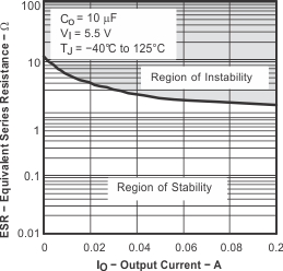
| COUT | Output capacitor | 2.2 | 10 | µF | |
| CNR | Noise reduction capacitor | 0 | 10 | nF | |
| CFF | Feed-forward capacitor | 15 | pF | ||
| R2 | Lower feedback resistor | 30.1 | kΩ | ||
7.4 Thermal Information
| THERMAL METRIC(1) | TPS793xx-Q1 | UNIT | |
|---|---|---|---|
| DBV (SOT-23) | |||
| 6 PINS | |||
| RθJA | Junction-to-ambient thermal resistance | 225.1 | °C/W |
| RθJC(top) | Junction-to-case (top) thermal resistance | 78.4 | °C/W |
| RθJB | Junction-to-board thermal resistance | 54.7 | °C/W |
| ψJT | Junction-to-top characterization parameter | 3.3 | °C/W |
| ψJB | Junction-to-board characterization parameter | 53.8 | °C/W |
| RθJC(bot) | Junction-to-case (bottom) thermal resistance | N/A | °C/W |
(1) For more information about traditional and new thermal metrics, see the Semiconductor and IC Package Thermal Metrics application report, SPRA953.
7.5 Electrical Characteristics
over recommended operating free-air temperature range, EN = VI, TJ = –40 to 125°C, VI = VO(typ) + 1 V, IO = 1 mA, Co = 10 μF, C(byp) = 0.01 μF (unless otherwise noted)| PARAMETER | TEST CONDITIONS | MIN | TYP | MAX | UNIT | |||
|---|---|---|---|---|---|---|---|---|
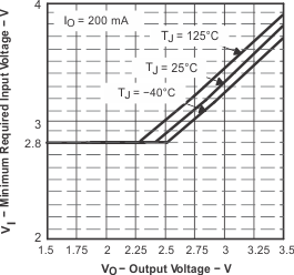
| VI | Input voltage(1) | 2.7 | 5.5 | V | ||||
| IO | Continuous output current | 0 | 200 | mA | ||||
| TJ | Operating junction temperature | –40 | 125 | °C | ||||
| Output voltage | TPS79301-Q1 | 0 μA < IO < 200 mA | VFB | 5.5 – VDROPOUT | V | |||
| TPS79318-Q1 | TJ = 25°C | 1.8 | ||||||
| 0 μA < IO < 200 mA, | 2.8 V < VI < 5.5 V | 1.764 | 1.836 | |||||
| TPS79325-Q1 | TJ = 25°C | 2.5 | ||||||
| 0 μA < IO < 200 mA, | 3.5 V < VI < 5.5 V | 2.45 | 2.55 | |||||
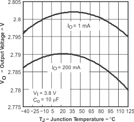
| TPS79328-Q1 | TJ = 25°C | 2.8 | ||||||
| 0 μA < IO < 200 mA, | 3.8 V < VI < 5.5 V | 2.744 | 2.856 | |||||
| TPS79330-Q1 | TJ = 25°C | 3 | ||||||
| 0 μA < IO < 200 mA, | 4 V < VI < 5.5 V | 2.94 | 3.06 | |||||
| TPS79333-Q1 | TJ = 25°C | 3.3 | ||||||
| 0 μA < IO < 200 mA, | 4.3 V < VI < 5.5 V | 3.234 | 3.366 | |||||
| TPS793475-Q1 | TJ = 25°C | 4.75 | ||||||
| 0 μA < IO < 200 mA, | 5.25 V < VI < 5.5 V | 4.655 | 4.845 | |||||
| Quiescent current (GND current) | 0 μA < IO < 200 mA, | TJ = 25°C | 170 | μA | ||||
| 0 μA < IO < 200 mA | 220 | |||||||
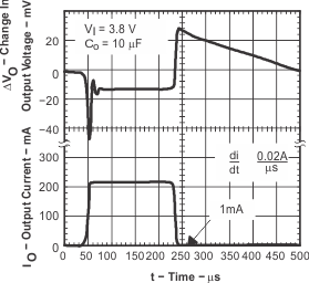
| Load regulation | 0 μA < IO < 200 mA, | TJ = 25°C | 5 | mV | ||||
| Output voltage line regulation (ΔVO/VO) | VO + 1 V < VI ≤ 5.5 V, | TJ = 25°C | 0.05 | %/V | ||||
| VO + 1 V < VI ≤ 5.5 V | 0.12 | |||||||
| Output noise voltage | TPS79328-Q1 | BW = 200 Hz to 100 kHz, IO = 200 mA, TJ = 25°C |
C(byp) = 0.001 μF | 55 | μVRMS | |||
| C(byp) = 0.0047 μF | 36 | |||||||
| C(byp) = 0.01 μF | 33 | |||||||
| C(byp) = 0.1 μF | 32 | |||||||
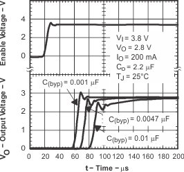
| Time, start-up | TPS79328-Q1 | RL = 14 Ω, Co = 1 μF, TJ = 25°C |
C(byp) = 0.001 μF | 50 | μs | |||
| C(byp) = 0.0047 μF | 70 | |||||||
| C(byp) = 0.01 μF | 100 | |||||||
| Output current limit | VO = 0 V | 285 | 600 | mA | ||||
| Standby current(3) | EN = 0 V, | 2.7 V < VI < 5.5 V | 0.07 | 1 | μA | |||
| High-level enable input voltage | 2.7 V < VI < 5.5 V | 2 | V | |||||
| Low-level enable input voltage | 2.7 V < VI < 5.5 V | 0.7 | V | |||||
| Input current (EN) | EN = 0 | –1 | 1 | μA | ||||
| Input current (FB) | TPS79301-Q1 | FB = 1.8 V | 1 | μA | ||||
| Internal reference, VFB | TPS79301-Q1 | 1.201 | 1.225 | 1.250 | V | |||
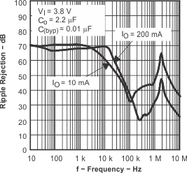
| Power-supply ripple rejection | TPS79328-Q1 | f = 100 Hz, TJ = 25°C, | IO = 10 mA | 70 | dB | |||
| IO = 200 mA | 68 | |||||||
| f = 10 kHz, TJ = 25°C, | IO = 200 mA | 70 | ||||||
| f = 100 kHz, TJ = 25°C, | 43 | |||||||
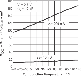
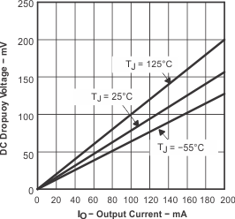
| Dropout voltage(2) | TPS79328-Q1 | IO = 200 mA, | TJ = 25°C | 120 | mV | |||
| IO = 200 mA | 200 | |||||||
| TPS79330-Q1 | IO = 200 mA, | TJ = 25°C | 112 | |||||
| IO = 200 mA | 200 | |||||||
| TPS79333-Q1 | IO = 200 mA, | TJ = 25°C | 102 | |||||
| IO = 200 mA | 180 | |||||||
| TPS793475-Q1 | IO = 200 mA, | TJ = 25°C | 77 | |||||
| IO = 200 mA | 125 | |||||||
| UVLO threshold | VCC rising | 2.25 | 2.65 | V | ||||
| UVLO hysteresis | TJ = 25°C | VCC rising | 100 | mV | ||||
(1) Minimum VIN is 2.7 V or VOUT + VDO, whichever is greater.
(2) Dropout is not measured for the TPS79318-Q1 and TPS79325-Q1 since minimum VIN = 2.7 V.
(3) For adjustable versions, this parameter applies only after VIN is applied; then VEN transitions high to low.
7.6 Typical Characteristics
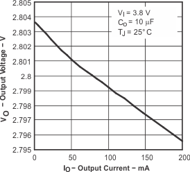
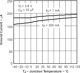
Junction Temperature
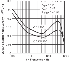
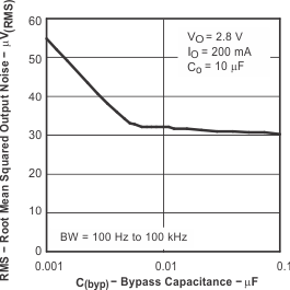
Bypass Capacitance
Junction Temperature
