SLVS348L July   2001  – May 2015 TPS793

PRODUCTION DATA.  

  1. Features
  2. Applications
  3. Description
  4. Revision History
  5. Pin Configuration and Functions
  6. Specifications
    1. 6.1 Absolute Maximum Ratings
    2. 6.2 ESD Ratings
    3. 6.3 Recommended Operating Conditions
    4. 6.4 Thermal Information
    5. 6.5 Electrical Characteristics
    6. 6.6 Typical Characteristics
  7. Detailed Description
    1. 7.1 Overview
    2. 7.2 Functional Block Diagrams
    3. 7.3 Feature Description
      1. 7.3.1 Undervoltage Lockout (UVLO)
      2. 7.3.2 Shutdown
      3. 7.3.3 Foldback Current Limit
      4. 7.3.4 Thermal Protection
      5. 7.3.5 Reverse Current Operation
    4. 7.4 Device Functional Modes
      1. 7.4.1 Normal Operation
      2. 7.4.2 Dropout Operation
      3. 7.4.3 Disabled
  8. Application and Implementation
    1. 8.1 Application Information
      1. 8.1.1 Adjustable Operation
    2. 8.2 Typical Application
      1. 8.2.1 Design Requirements
      2. 8.2.2 Detailed Design Procedure
        1. 8.2.2.1 Capacitor Recommendations
        2. 8.2.2.2 Input and Output Capacitor Requirements
        3. 8.2.2.3 Noise Reduction and Feed-Forward Capacitor Requirements
      3. 8.2.3 Application Curves
    3. 8.3 Do's and Don'ts
  9. Power Supply Recommendations
  10. 10Layout
    1. 10.1 Layout Guidelines
      1. 10.1.1 Board Layout Recommendations to Improve PSRR and Noise Performance
    2. 10.2 Layout Example
    3. 10.3 Power Dissipation
  11. 11Device and Documentation Support
    1. 11.1 Device Support
      1. 11.1.1 Development Support
        1. 11.1.1.1 Evaluation Modules
        2. 11.1.1.2 Spice Models
      2. 11.1.2 Device Nomenclature
    2. 11.2 Documentation Support
      1. 11.2.1 Related Documentation
    3. 11.3 Community Resource
    4. 11.4 Trademarks
    5. 11.5 Electrostatic Discharge Caution
    6. 11.6 Glossary
  12. 12Mechanical, Packaging, and Orderable Information
    1. 12.1 TPS793XXYEQ, YZQ Nanostar Wafer Chip Scale Information

封装选项

机械数据 (封装 | 引脚)
散热焊盘机械数据 (封装 | 引脚)
订购信息

5 Pin Configuration and Functions

DBV Package
5-Pin SOT-23 Fixed Voltage Version
Top View
TPS793 po_fixed_lvs348.gif
DBV Package
6-Pin SOT-23 Adjustable Voltage Version
Top View
TPS793 po_adjust_lvs348.gif
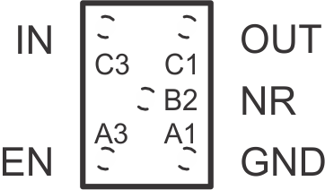
YZQ Package
5-Pin DSBGA
Top View
TPS793 po_yzq_lvs348.gif

Pin Functions

PIN I/O DESCRIPTION
NAME DBV YZQ
EN 3 A3 I Enable pin. Driving the enable pin (EN) high turns on the regulator. Driving this pin low puts the regulator into shutdown mode. EN can be connected to IN if not used.
FB 5 I Feedback pin. This terminal is the feedback input pin for the adjustable device. Fixed voltage versions in the DBV package do not have this pin.
GND 2 A1 Regulator ground.
IN 1 C3 I Input to the device.
NR 4 B2 Noise Reduction pin. Connecting an external capacitor to this pin filters noise generated by the internal bandgap. This configuration improves power-supply rejection and reduces output noise.
OUT 6 C1 O Output of the regulator.