ZHCSJN7J October 2002 – May 2019 TPS795
PRODUCTION DATA.
- 1 特性
- 2 应用
- 3 说明
- 4 修订历史记录
- 5 Pin Configuration and Functions
- 6 Specifications
- 7 Detailed Description
- 8 Application and Implementation
- 9 Power Supply Recommendations
- 10Layout
- 11器件和文档支持
- 12机械、封装和可订购信息
封装选项
机械数据 (封装 | 引脚)
散热焊盘机械数据 (封装 | 引脚)
- DRB|8
订购信息
10.1.3 Thermal Considerations
Knowing the device power dissipation and proper sizing of the thermal plane that is connected to the tab or pad is critical to avoiding thermal shutdown and ensuring reliable operation.
Power dissipation of the device depends on input voltage and load conditions and can be calculated using Equation 4:

Power dissipation can be minimized and greater efficiency can be achieved by using the lowest possible input voltage necessary to achieve the required output voltage regulation.
On the VSON (DRB) package, the primary conduction path for heat is through the exposed pad to the printed-circuit-board (PCB). The pad can be connected to ground or be left floating; however, it should be attached to an appropriate amount of copper PCB area to ensure the device does not overheat. On the SOT-223 (DCQ) package, the primary conduction path for heat is through the tab to the PCB. The tab should be connected to ground. The maximum junction-to-ambient thermal resistance depends on the maximum ambient temperature, maximum device junction temperature, and power dissipation of the device and can be calculated using Equation 5:

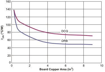
Knowing the maximum RθJA, the minimum amount of PCB copper area needed for appropriate heatsinking can be estimated using Figure 29.

NOTE:
θJA value at board size of 9 in.2 (that is, 3 in. × 3 in.) is a JEDEC standard.Figure 29 shows the variation of θJA as a function of ground plane copper area in the board. It is intended only as a guideline to demonstrate the effect of heat spreading in the ground plane and should not be used to estimate the thermal performance in real application environments.
NOTE
When the device is mounted on an application PCB, it is strongly recommended to use ΨJT and ΨJB, as explained in .