SLVS351P September 2002 – March 2015
PRODUCTION DATA.
- 1 Features
- 2 Applications
- 3 Description
- 4 Revision History
- 5 Pin Configuration and Functions
- 6 Specifications
- 7 Detailed Description
- 8 Application and Implementation
- 9 Power Supply Recommendations
- 10Layout
- 11Device and Documentation Support
- 12Mechanical, Packaging, and Orderable Information
封装选项
机械数据 (封装 | 引脚)
散热焊盘机械数据 (封装 | 引脚)
订购信息
7 Detailed Description
7.1 Overview
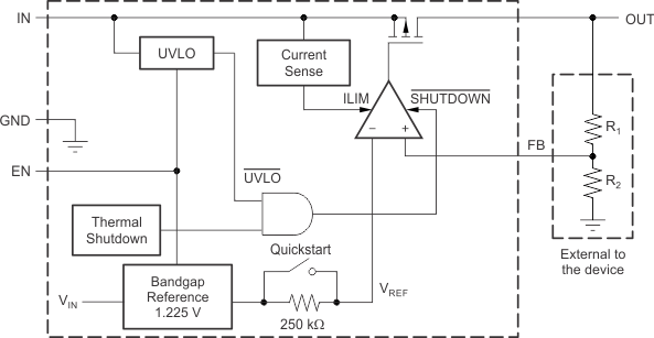
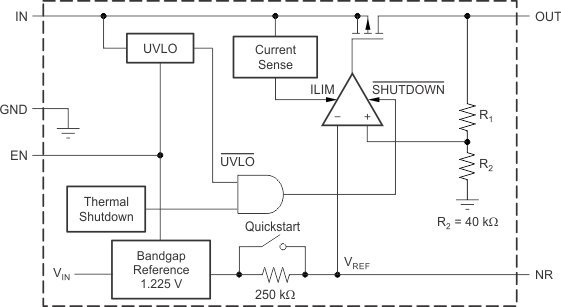
The TPS796 family of low-dropout (LDO) regulators combines the high performance required of many RF and precision analog applications with low current consumption. High PSRR is provided by a high-gain, high-bandwidth error loop with good supply rejection at very low headroom (VIN – VOUT). A noise-reduction pin is provided to bypass noise generated by the band-gap reference and to improve PSRR, while a quick-start circuit quickly charges this capacitor at start-up. All versions have thermal and overcurrent protection, and are fully specified from –40°C to 125°C.
7.2 Functional Block Diagrams
 Figure 22. Functional Block Diagram—Adjustable Version
 Figure 23. Functional Block Diagram—Fixed Version
7.3 Feature Description
7.3.1 Shutdown
The enable pin (EN) is active high and is compatible with standard and low-voltage TTL-CMOS levels. When shutdown capability is not required, EN can be connected to IN.
7.3.2 Start-Up
The TPS796 uses a start-up circuit to quickly charge the noise reduction capacitor, CNR, if present (see the Functional Block Diagrams). This circuit allows for the combination of very low output noise and fast start-up times. The NR pin is high impedance so a low leakage CNR capacitor must be used; most ceramic capacitors are appropriate for this configuration.
For the fastest start-up, apply VIN first, and then drive the enable pin (EN) high. If EN is tied to IN, start-up is somewhat slower. To ensure that CNR is fully charged during start-up, use a 0.1-μF or smaller capacitor.
7.3.3 Undervoltage Lockout (UVLO)
The TPS796 uses an undervoltage lockout circuit to keep the output shut off until internal circuitry is operating properly. The UVLO circuit has approximately 100 mV of hysteresis to help reject input voltage drops when the regulator first turns on.
7.3.4 Regulator Protection
The TPS796xx PMOS-pass transistor has a built-in back diode that conducts reverse current when the input voltage drops below the output voltage (for example, during power-down). Current is conducted from the output to the input and is not internally limited. If extended reverse voltage operation is anticipated, external limiting might be appropriate.
The TPS796xx features internal current limiting and thermal protection. During normal operation, the TPS796xx limits output current to approximately 2.8 A. When current limiting engages, the output voltage scales back linearly until the overcurrent condition ends. While current limiting is designed to prevent gross device failure, care should be taken not to exceed the power dissipation ratings of the package. If the temperature of the device exceeds approximately 165°C (Tsd), thermal-protection circuitry shuts it down. Once the device has cooled down to below approximately 140°C, regulator operation resumes.
7.4 Device Functional Modes
Table 1 provides a quick comparison between the normal, dropout, and disabled modes of operation.
Table 1. Device Functional Mode Comparison
| OPERATING MODE | PARAMETER | |||
|---|---|---|---|---|
| VIN | EN | IOUT | TJ | |
| Normal | VIN > VOUT(nom) + VDO | VEN > VEN(HI) | IOUT < ICL | TJ < TSD |
| Dropout | VIN < VOUT(nom) + VDO | VEN > VEN(HI) | IOUT < ICL | TJ < TSD |
| Disabled | — | VEN < VEN(LO) | — | TJ > TSD |
7.4.1 Normal Operation
The device regulates to the nominal output voltage under the following conditions:
- The input voltage is greater than the nominal output voltage plus the dropout voltage (VOUT(nom) + VDO).
- The enable voltage has previously exceeded the enable rising threshold voltage and not yet decreased below the enable falling threshold.
- The output current is less than the current limit (IOUT < ICL).
- The device junction temperature is less than the thermal shutdown temperature (TJ < TSD).
7.4.2 Dropout Operation
If the input voltage is lower than the nominal output voltage plus the specified dropout voltage, but all other conditions are met for normal operation, the device operates in dropout mode. In this mode, the output voltage tracks the input voltage. During this mode, the transient performance of the device becomes significantly degraded because the pass device is in a triode state and no longer controls the current through the LDO. Line or load transients in dropout can result in large output-voltage deviations.
7.4.3 Disabled
The device is disabled under the following conditions:
- The enable voltage is less than the enable falling threshold voltage or has not yet exceeded the enable rising threshold.
- The device junction temperature is greater than the thermal shutdown temperature (TJ > TSD).