SLVS351P September   2002  – March 2015

PRODUCTION DATA.  

  1. Features
  2. Applications
  3. Description
  4. Revision History
  5. Pin Configuration and Functions
  6. Specifications
    1. 6.1 Absolute Maximum Ratings
    2. 6.2 ESD Ratings
    3. 6.3 Recommended Operating Conditions
    4. 6.4 Thermal Information
    5. 6.5 Electrical Characteristics
    6. 6.6 Typical Characteristics
  7. Detailed Description
    1. 7.1 Overview
    2. 7.2 Functional Block Diagrams
    3. 7.3 Feature Description
      1. 7.3.1 Shutdown
      2. 7.3.2 Start-Up
      3. 7.3.3 Undervoltage Lockout (UVLO)
      4. 7.3.4 Regulator Protection
    4. 7.4 Device Functional Modes
      1. 7.4.1 Normal Operation
      2. 7.4.2 Dropout Operation
      3. 7.4.3 Disabled
  8. Application and Implementation
    1. 8.1 Application Information
    2. 8.2 Typical Application
      1. 8.2.1 Design Requirements
      2. 8.2.2 Detailed Design Procedure
        1. 8.2.2.1 Input and Output Capacitor Requirements
        2. 8.2.2.2 Output Noise
        3. 8.2.2.3 Dropout Voltage
        4. 8.2.2.4 Programming the TPS79601 Adjustable LDO Regulator
      3. 8.2.3 Application Curves
    3. 8.3 Do's and Don'ts
  9. Power Supply Recommendations
  10. 10Layout
    1. 10.1 Layout Guidelines
      1. 10.1.1 Board Layout Recommendation to Improve PSRR and Noise Performance
      2. 10.1.2 Regulator Mounting
    2. 10.2 Layout Examples
    3. 10.3 Thermal Considerations
    4. 10.4 Estimating Junction Temperature
  11. 11Device and Documentation Support
    1. 11.1 Device Support
      1. 11.1.1 Development Support
        1. 11.1.1.1 Evaluation Modules
        2. 11.1.1.2 Spice Models
      2. 11.1.2 Device Nomenclature
    2. 11.2 Documentation Support
      1. 11.2.1 Related Documentation
    3. 11.3 Related Links
    4. 11.4 Trademarks
    5. 11.5 Electrostatic Discharge Caution
    6. 11.6 Glossary
  12. 12Mechanical, Packaging, and Orderable Information

封装选项

机械数据 (封装 | 引脚)
散热焊盘机械数据 (封装 | 引脚)
订购信息

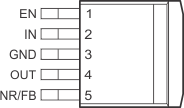
5 Pin Configuration and Functions

DCQ Package
6-Pin SOT-223
Top View
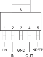
TPS79601 TPS79613 TPS79618 TPS79625 TPS79628 TPS79630 TPS79633 TPS79650 po_dcq_lvs351.gif
KTT Package
5-Pin TO-263
Top View
TPS79601 TPS79613 TPS79618 TPS79625 TPS79628 TPS79630 TPS79633 TPS79650 po_ktt_lvs351.gif
DRB Package
8-Pin VSON
Top View
TPS79601 TPS79613 TPS79618 TPS79625 TPS79628 TPS79630 TPS79633 TPS79650 po_drb_lvs351.gif

Pin Functions

PIN I/O DESCRIPTION
NAME SOT223
TO-263
VSON
EN 1 8 I Driving the enable pin (EN) high turns on the regulator. Driving this pin low puts the regulator into shutdown mode. EN can be connected to IN if not used.
FB 5 5 I This terminal is the feedback input voltage for the adjustable device.
GND 3, Tab 6, PowerPAD Regulator ground
IN 2 1, 2 I Unregulated input to the device.
N/C 7 Not internally connected. This pin must either be left open, or tied to GND.
NR 5 5 Connecting an external capacitor to this pin bypasses noise generated by the internal bandgap. This improves power-supply rejection and reduces output noise.
OUT 4 3, 4 O Output of the regulator.