ZHCSU17F March 2009 – April 2024 TPS798-Q1
PRODUCTION DATA
6.3.1 Adjustable Operation
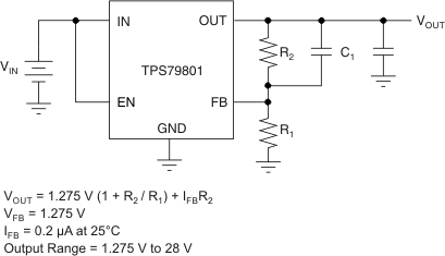
The TPS798-Q1 has an output voltage range of 1.275V to 28V. The output voltage is set by the ratio of two external resistors as shown in Figure 6-5. The feedback loop monitors the output to maintain the voltage at the adjust pin at 1.275V referenced to ground. The current in R1 is then equal to 1.275V / R1, and the current in R2 is the current in R1 plus the FB pin bias current. The FB pin bias current, 0.2μA at 25°C, flows through R2 into the FB pin. The output voltage can be calculated using the formula in Figure 6-5. The value of R1 must be less than 250kΩ to minimize errors in the output voltage caused by the FB pin bias current. When in shutdown, the output is turned off and the divider current is zero.
 Figure 6-5 Adjustable Operation
A 100pF capacitor (C1) placed in parallel with the top resistor (R2) of the output divider is necessary for stability and transient performance of the adjustable TPS798-Q1. The impedance of C1 at 10kHz must be less than the value of R2.
The adjustable device is tested and specified with the FB pin tied to the OUT pin and a 1mA DC load (unless otherwise specified) for an output voltage of 1.275V. Specifications for output voltages greater than 1.275V are proportional to the ratio of the desired output voltage to 1.275V (VOUT / 1.275V). For example, load regulation for an output current change of 1mA to 50mA is –10mV (typical) at VOUT = 1.275V.
At VOUT = 12V, load regulation is: