ZHCSIS2B september 2018 – december 2020 TPS7A11
PRODUCTION DATA
- 1
- 1 特性
- 2 应用
- 3 说明
- 4 Revision History
- 5 Pin Configuration and Functions
- 6 Specifications
- 7 Detailed Description
-
8 Application and Implementation
- 8.1
Application Information
- 8.1.1 Recommended Capacitor Types
- 8.1.2 Input and Output Capacitor Requirements
- 8.1.3 Load Transient Response
- 8.1.4 Dropout Voltage
- 8.1.5 Behavior During Transition From Dropout Into Regulation
- 8.1.6 Undervoltage Lockout Circuit Operation
- 8.1.7 Power Dissipation (PD)
- 8.1.8 Estimating Junction Temperature
- 8.1.9 Recommended Area for Continuous Operation
- 8.2 Typical Application
- 8.1
Application Information
- 9 Power Supply Recommendations
- 10Layout
- 11Device and Documentation Support
- Mechanical, Packaging, and Orderable Information
封装选项
机械数据 (封装 | 引脚)
散热焊盘机械数据 (封装 | 引脚)
- DRV|6
订购信息
8.1.9 Recommended Area for Continuous Operation
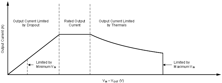
The operational area of an LDO is limited by the dropout voltage, output current, junction temperature, and input voltage. The recommended area for continuous operation for a linear regulator is shown in Figure 8-3 and can be separated into the following regions:
- Dropout voltage limits the minimum differential voltage between the input and the output (VIN – VOUT) at a given output current level; see the Dropout Voltage section for more details.
- The rated output current limits the maximum recommended output current level. Exceeding this rating causes the device to fall out of specification.
- The rated junction temperature limits the maximum junction temperature of the device. Exceeding this rating causes the device to fall out of specification and reduces long-term reliability.
- Equation 5 provides the shape of the slope. The slope is nonlinear because the maximum rated junction temperature of the LDO is controlled by the power dissipation across the LDO, thus when VIN – VOUT increases the output current must decrease.
- The rated input voltage range governs both the minimum and maximum of VIN – VOUT.
 Figure 8-3 Continuous Operation Diagram With Description of Regions