ZHCS237F December 2011 – October 2015 TPS7A16
PRODUCTION DATA.
- 1 特性
- 2 应用
- 3 说明
- 4 修订历史记录
- 5 Pin Configuration and Functions
- 6 Specifications
- 7 Detailed Description
- 8 Application and Implementation
- 9 Power Supply Recommendations
- 10Layout
- 11器件和文档支持
- 12机械、封装和可订购信息
封装选项
机械数据 (封装 | 引脚)
散热焊盘机械数据 (封装 | 引脚)
订购信息
10 Layout
10.1 Layout Guidelines
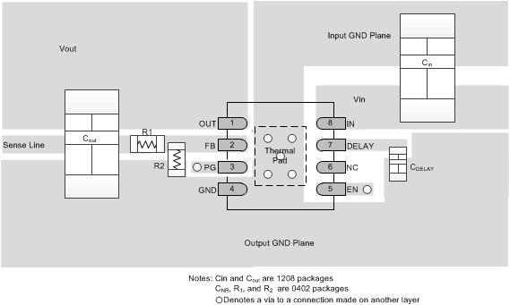
To improve AC performance such as PSRR, output noise, and transient response, it is recommended that the board be designed with separate ground planes for IN and OUT, with each ground plane connected only at the GND pin of the device. In addition, the ground connection for the output capacitor should connect directly to the GND pin of the device.
Equivalent series inductance (ESL) and ESR must be minimized in order to maximize performance and ensure stability. Every capacitor must be placed as close as possible to the device and on the same side of the PCB as the regulator itself.
Do not place any of the capacitors on the opposite side of the PCB from where the regulator is installed. The use of vias and long traces is strongly discouraged because they may impact system performance negatively and even cause instability.
If possible, and to ensure the maximum performance denoted in this product data sheet, use the same layout pattern used for TPS7A16 evaluation board, available at www.ti.com.
10.1.1 Additional Layout Considerations
The high impedance of the FB pin makes the regulator sensitive to parasitic capacitances that may couple undesirable signals from near-by components (specially from logic and digital ICs, such as microcontrollers and microprocessors); these capacitively-coupled signals may produce undesirable output voltage transients. In these cases, TI recommends using a fixed-voltage version of the TPS7A16, or isolate the FB node by flooding the local PCB area with ground-plane copper to minimize any undesirable signal coupling.
10.2 Layout Example
Layout is a critical part of good power-supply design. There are several signal paths that conduct fast-changing currents or voltages that can interact with stray inductance or parasitic capacitance to generate noise or degrade the power-supply performance. To help eliminate these problems, the IN pin should be bypassed to ground with a low ESR ceramic bypass capacitor with a X5R or X7R dielectric.
It may be possible to obtain acceptable performance with alternative PCB layouts; however, the layout and the schematic have been shown to produce good results and are meant as a guideline.
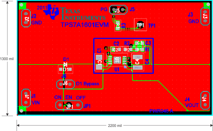
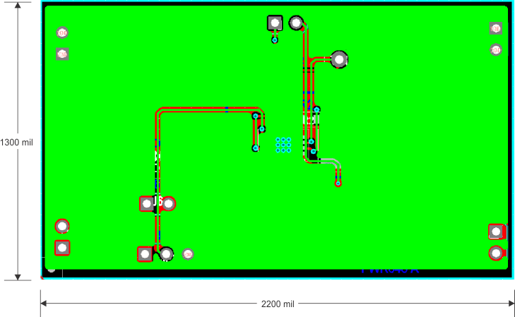
Figure 21 shows the schematic for the suggested layout. Figure 22 and Figure 23 show the top and bottom printed-circuit-board (PCB) layers for the suggested layout.
 Figure 21. Schematic for Suggested Layout
 Figure 22. Suggested Layout: Top Layer
 Figure 23. Suggested Layout: Bottom Layer
10.3 Power Dissipation
The ability to remove heat from the die is different for each package type, presenting different considerations in the PCB layout. The PCB area around the device that is free of other components moves the heat from the device to the ambient air. Using heavier copper increases the effectiveness in removing heat from the device. The addition of plated through-holes to heat dissipating layers also improves the heatsink effectiveness.
Power dissipation depends on input voltage and load conditions. Power dissipation (PD) is equal to the product of the output current times the voltage drop across the output pass element, as shown in Equation 2:

10.4 Thermal Considerations
Any tendency to activate the thermal protection circuit indicates excessive power dissipation or an inadequate heat spreading area. For reliable operation, junction temperature should be limited to a maximum of +125°C at the worst case ambient temperature for a given application. To estimate the margin of safety in a complete design (including the copper heat-spreading area), increase the ambient temperature until the thermal protection is triggered; use worst-case loads and signal conditions. For good reliability, thermal protection should trigger at least +45°C above the maximum expected ambient condition of the particular application. This configuration produces a worst-case junction temperature of +125°C at the highest expected ambient temperature and worst-case load.
The internal protection circuitry of the TPS7A16 has been designed to protect against overload conditions. It was not intended to replace proper heatsinking. Continuously running the TPS7A16 into thermal shutdown degrades device reliability.