ZHCSFK0A May   2016  – September 2016 TPS7A19

PRODUCTION DATA.  

  1. 特性
  2. 应用范围
  3. 说明
  4. 修订历史记录
  5. Pin Configuration and Functions
  6. Specifications
    1. 6.1 Absolute Maximum Ratings
    2. 6.2 ESD Ratings
    3. 6.3 Recommended Operating Conditions
    4. 6.4 Thermal Information
    5. 6.5 Electrical Characteristics
    6. 6.6 Timing Requirements
    7. 6.7 Typical Characteristics
  7. Detailed Description
    1. 7.1 Overview
    2. 7.2 Functional Block Diagram
    3. 7.3 Feature Description
      1. 7.3.1 Enable Pin (EN)
      2. 7.3.2 Regulated Output Pin (OUT)
      3. 7.3.3 Power-Good Pin (PG)
      4. 7.3.4 Delay Timer Pin (DELAY)
      5. 7.3.5 Adjustable Output Voltage (ADJ for TPS7A1901)
      6. 7.3.6 Undervoltage Shutdown
      7. 7.3.7 Thermal Shutdown
    4. 7.4 Device Functional Modes
      1. 7.4.1 Operation With VIN < 4 V
      2. 7.4.2 Operation With EN Control
  8. Application and Implementation
    1. 8.1 Application Information
    2. 8.2 Typical Application
      1. 8.2.1 Design Requirements
      2. 8.2.2 Detailed Design Procedure
        1. 8.2.2.1 Power Dissipation and Thermal Considerations
      3. 8.2.3 Application Curves
  9. Power Supply Recommendations
  10. 10Layout
    1. 10.1 Layout Guidelines
    2. 10.2 Layout Example
  11. 11器件和文档支持
    1. 11.1 器件支持
      1. 11.1.1 开发支持
        1. 11.1.1.1 评估模块
        2. 11.1.1.2 Spice 模型
      2. 11.1.2 器件命名规则
    2. 11.2 文档支持
      1. 11.2.1 相关文档
    3. 11.3 接收文档更新通知
    4. 11.4 社区资源
    5. 11.5 商标
    6. 11.6 静电放电警告
    7. 11.7 Glossary
  12. 12机械、封装和可订购信息

封装选项

机械数据 (封装 | 引脚)
散热焊盘机械数据 (封装 | 引脚)
订购信息

Layout

Layout Guidelines

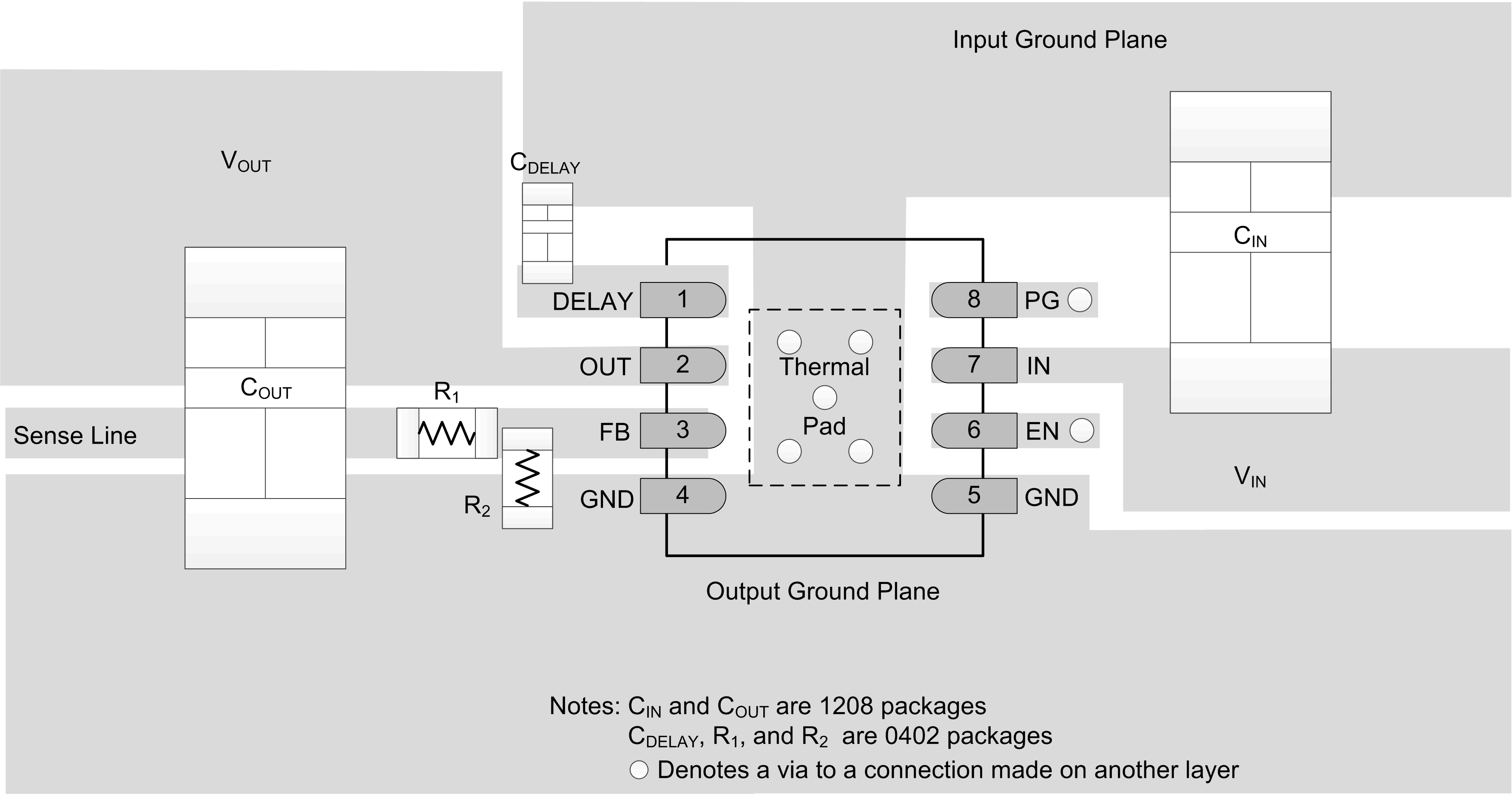
  • To improve ac performance such as PSRR, output noise, and transient response, design the board with separate ground planes for VIN and VOUT, with each ground plane connected only at the GND pin of the device. In addition, connect the ground connection for the output capacitor directly to the GND pin of the device.
  • Minimize equivalent series inductance (ESL) and equivalent series resistance (ESR) in order to maximize performance and stability. Place every capacitor as close to the device as possible, and on the same side of the PCB as the regulator.
  • Do not place any of the capacitors on the opposite side of the PCB from where the regulator is installed. The use of vias and long traces are strongly discouraged because of the negative impact on system performance. Vias and long traces can also cause instability.
  • If possible, and to maximize the performance listed in this data sheet, use the same layout pattern used for the TPS7A19 evaluation module, TPS7A1901EVM-760 (SBVU031).

Layout Example

TPS7A19 layout_example_sbvs256.gif Figure 16. TPS7A19 Layout Example