ZHCSJ50C December 2018 – December 2022 TPS7A25
PRODUCTION DATA
- 1 特性
- 2 应用
- 3 说明
- 4 Revision History
- 5 Pin Configuration and Functions
- 6 Specifications
- 7 Typical Characteristics
-
8 Detailed Description
- 8.1 Overview
- 8.2 Functional Block Diagrams
- 8.3 Feature Description
- 8.4 Device Functional Modes
- 9 Device and Documentation Support
- 10Mechanical, Packaging, and Orderable Information
封装选项
请参考 PDF 数据表获取器件具体的封装图。
机械数据 (封装 | 引脚)
- DRV|6
散热焊盘机械数据 (封装 | 引脚)
- DRV|6
订购信息
9.1.4 Reverse Current
Excessive reverse current can damage this device. Reverse current flows through the intrinsic body diode of the pass transistor instead of the normal conducting channel. At high magnitudes, this current flow degrades the long-term reliability of the device.
Conditions where reverse current can occur are outlined in this section, all of which can exceed the absolute maximum rating of VOUT ≤ VIN + 0.3 V.
- If the device has a large COUT and the input supply collapses with little or no load current
- The output is biased when the input supply is not established
- The output is biased above the input supply
If reverse current flow is expected in the application, external protection is recommended to protect the device. Reverse current is not limited in the device, so external limiting is required if extended reverse voltage operation is anticipated.
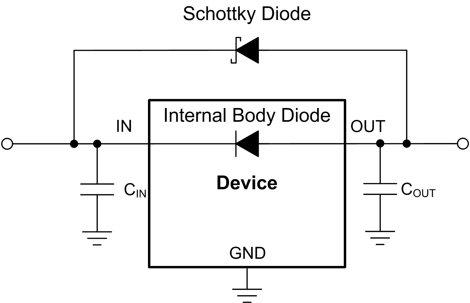
Figure 9-1 shows one approach for protecting the device.
 Figure 9-1 Example
Circuit for Reverse Current Protection Using a Schottky Diode
Figure 9-1 Example
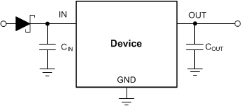
Circuit for Reverse Current Protection Using a Schottky DiodeFigure 9-2 shows another, more commonly used, approach in high input voltage applications.
 Figure 9-2 Reverse Current Prevention Using A Diode Before the LDO