ZHCSHP4B December   2018  – October 2019 TPS7A26

PRODUCTION DATA.  

  1. 特性
  2. 应用
  3. 说明
    1.     Device Images
      1.      典型应用电路
  4. 修订历史记录
  5. Pin Configuration and Functions
    1.     Pin Functions
  6. Specifications
    1. 6.1 Absolute Maximum Ratings
    2. 6.2 ESD Ratings
    3. 6.3 Recommended Operating Conditions
    4. 6.4 Thermal Information
    5. 6.5 Electrical Characteristics
    6. 6.6 Typical Characteristics
  7. Detailed Description
    1. 7.1 Overview
    2. 7.2 Functional Block Diagram
    3. 7.3 Feature Description
      1. 7.3.1 Output Enable
      2. 7.3.2 Dropout Voltage
      3. 7.3.3 Current Limit
      4. 7.3.4 Undervoltage Lockout (UVLO)
      5. 7.3.5 Thermal Shutdown
      6. 7.3.6 Power Good
      7. 7.3.7 Active Overshoot Pulldown Circuitry
    4. 7.4 Device Functional Modes
      1. 7.4.1 Device Functional Mode Comparison
      2. 7.4.2 Normal Operation
      3. 7.4.3 Dropout Operation
      4. 7.4.4 Disabled
  8. Application and Implementation
    1. 8.1 Application Information
      1. 8.1.1 Adjustable Device Feedback Resistors
      2. 8.1.2 Recommended Capacitor Types
      3. 8.1.3 Input and Output Capacitor Requirements
      4. 8.1.4 Reverse Current
      5. 8.1.5 Feed-Forward Capacitor (CFF)
      6. 8.1.6 Power Dissipation (PD)
      7. 8.1.7 Estimating Junction Temperature
      8. 8.1.8 Special Consideration for Line Transient
    2. 8.2 Typical Application
      1. 8.2.1 Design Requirements
      2. 8.2.2 Detailed Design Procedure
        1. 8.2.2.1 Transient Response
        2. 8.2.2.2 Selecting Feedback Divider Resistors
        3. 8.2.2.3 Thermal Dissipation
      3. 8.2.3 Application Curve
  9. Power Supply Recommendations
  10. 10Layout
    1. 10.1 Layout Guidelines
    2. 10.2 Layout Examples
  11. 11器件和文档支持
    1. 11.1 器件支持
      1. 11.1.1 器件命名规则
    2. 11.2 文档支持
      1. 11.2.1 相关文档
    3. 11.3 接收文档更新通知
    4. 11.4 社区资源
    5. 11.5 商标
    6. 11.6 静电放电警告
    7. 11.7 Glossary
  12. 12机械、封装和可订购信息

封装选项

请参考 PDF 数据表获取器件具体的封装图。

机械数据 (封装 | 引脚)
  • DRV|6
散热焊盘机械数据 (封装 | 引脚)
订购信息

Special Consideration for Line Transient

During a line transient, the response of this LDO to a very large or fast input voltage change can cause a brief shutdown lasting up to a few hundred microseconds from the voltage transition. This shutdown can be avoided by reducing the voltage step size, increasing the transition time, or a combination of both. Figure 39 provides a boundary to follow to avoid this behavior. If necessary, reduce slew rate and the voltage step size to stay below the curve.
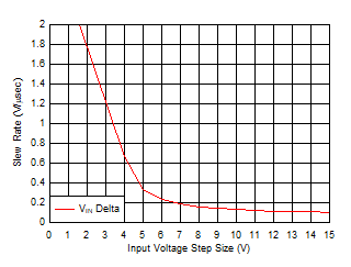
TPS7A26 D043_SBVS290.gifFigure 39. Recommended Input Voltage Step and Slew Rate in a Line transient