SBVS125D August 2010 – June 2015 TPS7A30
PRODUCTION DATA.
- 1 Features
- 2 Applications
- 3 Description
- 4 Revision History
- 5 Pin Configuration and Functions
- 6 Specifications
- 7 Parameter Measurement Information
- 8 Detailed Description
-
9 Application and Implementation
- 9.1 Application Information
- 9.2 Typical Application
- 9.3 Do's and Don’ts
- 10Power Supply Recommendations
- 11Layout
- 12Device and Documentation Support
- 13Mechanical, Packaging, and Orderable Information
封装选项
机械数据 (封装 | 引脚)
散热焊盘机械数据 (封装 | 引脚)
订购信息
8 Detailed Description
8.1 Overview
The TPS7A30 family of devices are wide VIN, low-noise, 150-mA linear regulators (LDOs). These devices feature an enable pin, programmable soft-start, current limiting, and thermal protection circuitry that allow the device to be used in a wide variety of applications. As bipolar-based devices, the TPS7A30 devices are ideal for high-accuracy, high-precision applications at higher voltages.
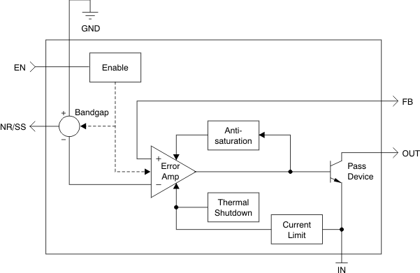
8.2 Functional Block Diagram

8.3 Feature Description
8.3.1 Internal Current Limit
The fixed internal current limit of the TPS7A30 family helps protect the regulator during fault conditions. The maximum amount of current the device can source is the current limit (330 mA, typical), and is largely independent of the output voltage. For reliable operation, do not operate the device in current limit for extended periods of time.
8.3.2 Programmable Soft-Start
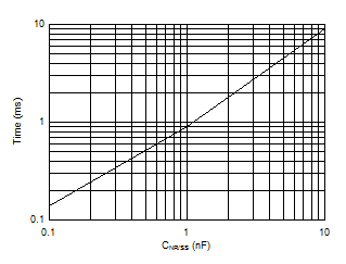
The NR/SS capacitor also functions as a soft-start capacitor to slow down the rise time of the output. The rise time of the output when using an NR/SS capacitor is governed by Equation 1. In Equation 1, tSS is the soft-start time in milliseconds and CNR/SS is the capacitance at the NR pin in nanofarads. Figure 29 shows the relationship between the CNR/SS size and the start-up time without a CFF.

 Figure 29. Soft-Start Time vs CNR/SS
8.3.3 Enable Pin Operation
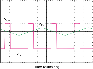
The TPS7A30 provides a dual-polarity enable pin (EN) that turns on the regulator when |VEN| > 2 V, whether the voltage is positive or negative, as shown in Figure 30.
This functionality allows for different system power management topologies:
- Connecting the EN pin directly to a negative voltage (such as VIN).
- Connecting the EN pin directly to a positive voltage, such as the output of digital logic circuitry.
 Figure 30. Enable Pin Positive and Negative Threshold
8.4 Device Functional Modes
8.4.1 Normal Operation
The device regulates to the nominal output voltage under the following conditions:
- The input voltage is at least as high as the |VIN(min)|.
- The input voltage magnitude is greater than the nominal output voltage magnitude added to the dropout voltage.
- |VEN| > |V(HI)|.
- The output current is less than the current limit.
- The device junction temperature is less than the maximum specified junction temperature.
8.4.2 Dropout Operation
If the input voltage magnitude is lower than the nominal output voltage magnitude plus the specified dropout voltage magnitude, but all other conditions are met for normal operation, the device operates in dropout mode. In this mode of operation, the output voltage magnitude is the same as the input voltage magnitude minus the dropout voltage magnitude. The transient performance of the device is significantly degraded because the pass device (such as a bipolar junction transistor, or BJT) is in saturation and no longer controls the current through the LDO. Line or load transients in dropout can result in large output voltage deviations.
8.4.3 Disabled
The device is disabled under the following conditions:
- |VEN| < |V(HI)|.
- The device junction temperature is greater than the thermal shutdown temperature.
Table 1 shows the conditions that lead to the different modes of operation.