ZHCSBQ0B July 2013 – March 2015 TPS7A3501
PRODUCTION DATA.
- 1 特性
- 2 应用
- 3 说明
- 4 修订历史记录
- 5 Pin Configuration and Functions
- 6 Specifications
- 7 Detailed Description
- 8 Application and Implementation
- 9 Power Supply Recommendations
- 10Layout
- 11器件和文档支持
- 12机械封装和可订购信息
8 Application and Implementation
NOTE
Information in the following applications sections is not part of the TI component specification, and TI does not warrant its accuracy or completeness. TI’s customers are responsible for determining suitability of components for their purposes. Customers should validate and test their design implementation to confirm system functionality.
8.1 Application Information
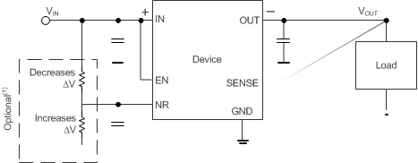
The TPS7A3501 is well-suited for use as a filter for switching power supplies. The high PSRR of the device significantly reduces the ripple caused by the switching frequency as well as the subsequent harmonic frequencies. Figure 21 shows the basic circuit connections for the TPS7A3501. The IN pin should be connected to a well-regulated power source, typically a switching power supply.
8.2 Typical Application
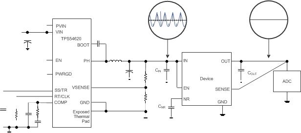
Figure 22 shows a schematic for filtering the output of a switching regulator using the TPS7A3501 to power an analog-to-digital converter (ADC).
 Figure 22. Typical Application Schematic
8.2.1 Design Requirements
Table 3 shows the design requirements.
Table 3. Design Requirements
| PARAMETER | DESIGN REQUIREMENT |
|---|---|
| Input voltage | 3.63 V |
| Output voltage | 3.3 V |
| 100-Hz to 100-kHz RMS noise | < 4 µVRMS |
| Maximum output current | 700 mA |
8.2.2 Detailed Design Procedure
Select the input and output capacitors to be at least 10 µF for stability. Select a value for RNR to give the desired voltage drop. For this example of a 330-mV voltage drop, no external resistor on the NR pin is required. Pick a value for CNR greater than 10 nF, but large enough to provide the required noise performance. Refer to Table 5 for guidelines on selecting CNR for a desired RMS noise target. For this example, to achieve an RMS noise (100 Hz to 100 kHz) less than 4 µVRMS, the noise reduction capacitor must be at least 1 µF.
8.2.2.1 Adjustable Voltage Drop
In the TPS7A3501, the nominal voltage drop (ΔV) from IN to OUT is 330 mV. ΔV can be adjusted from this nominal setting with an external resistor. By connecting a resistor from the NR pin to IN, ΔV can be decreased to as low as 200 mV. By connecting a resistor from the NR pin to GND, ΔV can be increased to as high as 500 mV. The ability to change ΔV allows for the creation of standard voltage rails from higher voltage rails (for example, 2.5 V from 3 V, 1.5 V from 1.8 V, and so forth).
By connecting a resistor from the NR pin to IN, ΔV can be decreased to as low as 200 mV. Use Equation 1 to determine the size of the resistor required to set ΔV.
By connecting a resistor from the NR pin to GND, ΔV can be increased to as high as 500 mV. Use Equation 2 to determine the size of the resistor required to set ΔV.
Table 4 lists the standard external resistor values required for different input-to-output voltage drops.
Table 4. Common Input-to-Output Voltage Drops
| ΔV (mV) | VOUT | R TO VIN | R TO GND |
|---|---|---|---|
| 200 | Any | 240 kΩ | Do not install |
| 330 | Any | Do not install | Do not install |
| 400 | 3.3 V | Do not install | 6.8 MΩ |
| 2.5 V | Do not install | 5.1 MΩ | |
| 1.8 V | Do not install | 3.9 MΩ | |
| 500 | 3.3 V | Do not install | 3 MΩ |
| 2.5 V | Do not install | 2.2 MΩ | |
| 1.8 V | Do not install | 1.6 MΩ |
8.2.2.2 Input and Output Capacitor Requirements
Ceramic 10-µF or larger input and output capacitors are required to assure proper device operation. This capacitor counteracts reactive source impedances, improving supply transient response and decreasing input ripple. Higher-value capacitors may be used if large, fast slew rate load transients are anticipated, or if the device is located several inches away from the power source. To assure correct device operation, there should be no more than 100 µF of capacitance on the output of the device, including capacitance from downstream bypass capacitors.
TI recommends X5R- and X7R-type ceramic capacitors because these types of capacitors have minimal variation in value and equivalent series resistance (ESR) overtemperature. Other types of capacitors, such as electrolytic or tantalum, can make the device unstable.
8.2.2.3 Output Noise
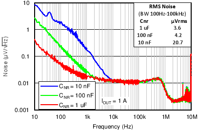
A 10-nF, or higher, noise-reduction capacitor is required to assure stability. Using a 1-μF ceramic capacitor minimizes output noise (see Figure 13). To assure correct device operation, a maximum capacitor of 2.2 µF can be connected to NR.
8.2.2.4 Power-Supply Rejection Ratio (PSRR)
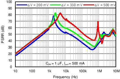
Unlike standard LDOs, the TPS7A3501 PSRR is significantly affected by the noise-reduction capacitor. The larger the noise-reduction capacitor, the higher the PSRR is for frequencies below 10 kHz. Using a 1-μF ceramic capacitor maximizes PSRR.
One of the most compelling features of the TPS7A3501 is its high PSRR capabilities. The rejection ratio for this device is lower than standard LDOs at frequencies below 1 kHz but becomes higher at higher frequencies. For better low-frequency PSRR performance, a larger noise-reduction capacitor can be used. TI recommends connecting a 1-µF ceramic capacitor to NR to maximize PSRR (see Figure 12). A higher input-to-output voltage difference also increases the device rejection ratio. Although the device maximizes rejection ratio at 500 mV, high rejection ratio can still be achieved with as little as a 330-mV input-to-output voltage differential, unlike most standard LDOs.
8.2.2.5 Start-up
Because adding a noise-reduction capacitor leads to the formation of an RC filter, start-up time and the rate at which the device tracks VIN are increased. Thus, consider the tradeoff between start-up time, noise, and PSRR when selecting a noise-reduction capacitor to use with the TPS7A3501. Use Equation 3 to calculate the typical start-up time.
Table 5 shows the effect of various noise-reduction capacitors on RMS noise (with a 100-Hz to 100-kHz bandwidth), PSRR (at 1 kHz), and start-up time.
Table 5. Effect of Various Filter Capacitors
| FILTER CAPACITOR | RMS NOISE (BW 100 Hz to 100 kHz) |
PSRR (at 1 kHz) |
START-UP TIME (EN to 90% of VOUT) |
|---|---|---|---|
| 1 µF | 3.62 µV | 60 dB | 250 ms |
| 100 nF | 4.21 µV | 40 dB | 25 ms |
| 10 nF | 20.70 µV | 20 dB | 3 ms |
8.2.2.6 Transient Response
Increasing the size of the output capacitor reduces overshoot and undershoot magnitude during transients; however this size increase also slows the recovery from these transients.
8.2.3 Application Curves
 Figure 23. Power-Supply Rejection Ratio vs Frequency
 Figure 24. Spectral Noise Density vs Frequency
8.3 Do's and Don'ts
Place at least 10-μF ceramic capacitors on both the IN and OUT pins of the device, as close as possible to the pins of the regulator.
Do not place the input or output capacitor more than 10 mm away from the regulator.
Connect a 10-nF or greater, low-equivalent series resistance (ESR) capacitor across the NR pin and GND of the regulator. Larger capacitors provide lower noise performance.
Do not use a capacitor larger than 2.2 µF on the NR pin.
Do not exceed the absolute maximum ratings.
