ZHCSGP0A July   2017  – September 2017 TPS7A39

PRODUCTION DATA.  

  1. 特性
  2. 应用
  3. 说明
  4. 修订历史记录
  5. Pin Configuration and Functions
  6. Specifications
    1. 6.1 Absolute Maximum Ratings
    2. 6.2 ESD Ratings
    3. 6.3 Recommended Operating Conditions
    4. 6.4 Thermal Information
    5. 6.5 Electrical Characteristics
    6. 6.6 Startup Characteristics
    7. 6.7 Typical Characteristics
  7. Detailed Description
    1. 7.1 Overview
    2. 7.2 Functional Block Diagram
    3. 7.3 Feature Description
      1. 7.3.1 Voltage Regulation
        1. 7.3.1.1 DC Regulation
        2. 7.3.1.2 AC and Transient Response
      2. 7.3.2 User-Settable Buffered Reference
      3. 7.3.3 Active Discharge
      4. 7.3.4 System Start-Up Controls
        1. 7.3.4.1 Start-Up Tracking
        2. 7.3.4.2 Sequencing
          1. 7.3.4.2.1 Enable (EN)
          2. 7.3.4.2.2 Undervoltage Lockout (UVLO) Control
    4. 7.4 Device Functional Modes
      1. 7.4.1 Normal Operation
      2. 7.4.2 Dropout Operation
      3. 7.4.3 Disabled
  8. Application and Implementation
    1. 8.1 Application Information
      1. 8.1.1  Setting the Output Voltages on Adjustable Devices
      2. 8.1.2  Capacitor Recommendations
      3. 8.1.3  Input and Output Capacitor (CINx and COUTx)
      4. 8.1.4  Feed-Forward Capacitor (CFFx)
      5. 8.1.5  Noise-Reduction and Soft-Start Capacitor (CNR/SS)
      6. 8.1.6  Buffered Reference Voltage
      7. 8.1.7  Overriding Internal Reference
      8. 8.1.8  Start-Up
        1. 8.1.8.1 Soft-Start Control (NR/SS)
          1. 8.1.8.1.1 In-Rush Current
        2. 8.1.8.2 Undervoltage Lockout (UVLOx) Control
      9. 8.1.9  AC and Transient Performance
        1. 8.1.9.1 Power-Supply Rejection Ratio (PSRR)
        2. 8.1.9.2 Channel-to-Channel Output Isolation and Crosstalk
        3. 8.1.9.3 Output Voltage Noise
        4. 8.1.9.4 Optimizing Noise and PSRR
        5. 8.1.9.5 Load Transient Response
      10. 8.1.10 DC Performance
        1. 8.1.10.1 Output Voltage Accuracy (VOUTx)
        2. 8.1.10.2 Dropout Voltage (VDO)
      11. 8.1.11 Reverse Current
      12. 8.1.12 Power Dissipation (PD)
        1. 8.1.12.1 Estimating Junction Temperature
    2. 8.2 Typical Applications
      1. 8.2.1 Design 1: Single-Ended to Differential Isolated Supply
        1. 8.2.1.1 Design Requirements
        2. 8.2.1.2 Detailed Design Procedure
          1. 8.2.1.2.1 Switcher Choice
          2. 8.2.1.2.2 Full Bridge Rectifier With Center-Tapped Transformer
          3. 8.2.1.2.3 Total Solution Efficiency
          4. 8.2.1.2.4 Feedback Resistor Selection
        3. 8.2.1.3 Application Curves
      2. 8.2.2 Design 2: Getting the Full Range of a SAR ADC
        1. 8.2.2.1 Design Requirements
        2. 8.2.2.2 Detailed Design Procedure
        3. 8.2.2.3 Detailed Design Description
          1. 8.2.2.3.1 Regulation of -0.2 V
          2. 8.2.2.3.2 Feedback Resistor Selection
        4. 8.2.2.4 Application Curves
  9. Power-Supply Recommendations
  10. 10Layout
    1. 10.1 Layout Guidelines
      1. 10.1.1 Board Layout Recommendations to Improve PSRR and Noise Performance
    2. 10.2 Layout Example
    3. 10.3 Package Mounting
  11. 11器件和文档支持
    1. 11.1 器件支持
      1. 11.1.1 开发支持
        1. 11.1.1.1 评估模块
        2. 11.1.1.2 Spice 模型
    2. 11.2 文档支持
      1. 11.2.1 相关文档
    3. 11.3 接收文档更新通知
    4. 11.4 社区资源
    5. 11.5 商标
    6. 11.6 静电放电警告
    7. 11.7 Glossary
  12. 12机械、封装和可订购信息

封装选项

机械数据 (封装 | 引脚)
散热焊盘机械数据 (封装 | 引脚)
订购信息

Layout

Layout Guidelines

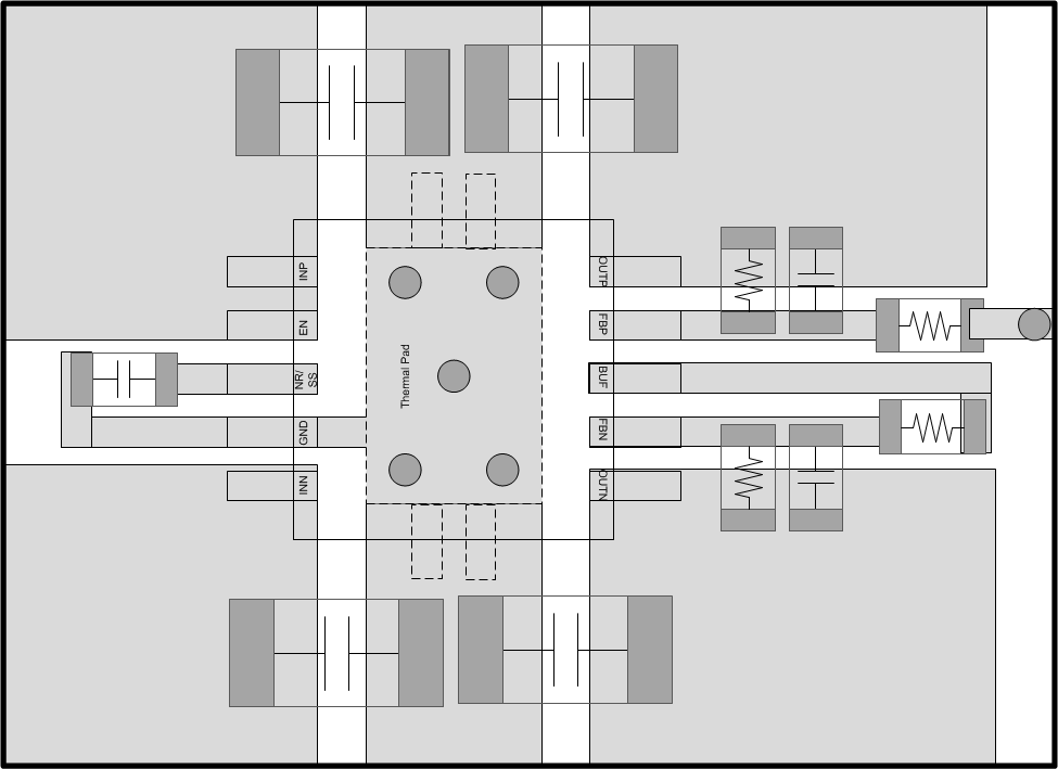
Layout is a critical part of good power-supply design. There are several signal paths that conduct fast-changing currents or voltages that can interact with stray inductance or parasitic capacitance to generate noise or degrade the power-supply performance. To help eliminate these problems, bypass the IN pin to ground with capacitors.

Tie the GND pin directly to the thermal pad under the device. The thermal pad must be connected to any internal PCB ground planes using multiple vias directly under the device.

Every capacitor must be placed as close as possible to the device and on the same side of the PCB as the regulator itself.

Do not place any of the capacitors on the opposite side of the PCB from where the regulator is installed. The use of vias and long traces is strongly discouraged because these circuits can impact system performance negatively, and even cause instability.

Board Layout Recommendations to Improve PSRR and Noise Performance

To improve ac performance (such as PSRR, output noise, and transient response), TI recommends that the board be designed with separate ground planes for VIN and VOUT, with each ground plane star connected only at the GND pin of the device. In addition, the ground connection for the bypass capacitor must connect directly to the GND pin of the device.

Layout Example

TPS7A39 Adjustable_DRC_Layout.gif Figure 81. Layout Example for Adjustable Option

Package Mounting

Solder pad footprint recommendations for the TPS7A39 are available at the end of this document and at www.ti.com.