ZHCSGP0A July 2017 – September 2017 TPS7A39
PRODUCTION DATA.
- 1 特性
- 2 应用
- 3 说明
- 4 修订历史记录
- 5 Pin Configuration and Functions
- 6 Specifications
- 7 Detailed Description
-
8 Application and Implementation
- 8.1
Application Information
- 8.1.1 Setting the Output Voltages on Adjustable Devices
- 8.1.2 Capacitor Recommendations
- 8.1.3 Input and Output Capacitor (CINx and COUTx)
- 8.1.4 Feed-Forward Capacitor (CFFx)
- 8.1.5 Noise-Reduction and Soft-Start Capacitor (CNR/SS)
- 8.1.6 Buffered Reference Voltage
- 8.1.7 Overriding Internal Reference
- 8.1.8 Start-Up
- 8.1.9 AC and Transient Performance
- 8.1.10 DC Performance
- 8.1.11 Reverse Current
- 8.1.12 Power Dissipation (PD)
- 8.2 Typical Applications
- 8.1
Application Information
- 9 Power-Supply Recommendations
- 10Layout
- 11器件和文档支持
- 12机械、封装和可订购信息
6 Specifications
6.1 Absolute Maximum Ratings
over operating junction temperature range (unless otherwise noted)(1)(2)| MIN | MAX | UNIT | ||
|---|---|---|---|---|
| Voltage | INP | –0.3 | 36 | V |
| INN | –36 | 0.3 | ||
| OUTP | –0.3 | VINP + 0.3(5) | ||
| OUTN | VINN – 0.3(4) | 0.3 | ||
| FBP | –0.3 | VINP + 0.3(7) | ||
| BUF | –1 | VINP + 0.3(7) | ||
| NR/SS | –0.3 | VINP + 0.3(8) | ||
| FBN | VINN – 0.3(3) | 0.3 | ||
| EN | –0.3 | VINP + 0.3(6) | ||
| Current | Output current | Internally limited | ||
| Buffer current | 2 | mA | ||
| Temperature | Operating junction temperature, TJ | –55 | 150 | °C |
| Storage, Tstg | –65 | 150 | ||
(1) Stresses beyond those listed under Absolute Maximum Ratings may cause permanent damage to the device. These are stress ratings only, which do not imply functional operation of the device at these or any other conditions beyond those indicated under Recommended Operating Conditions. Exposure to absolute-maximum-rated conditions for extended periods may affect device reliability.
(2) All voltages with respect to the ground pin, unless otherwise noted.
(3) The absolute maximum rating is VINN – 0.3 V or –3 V, whichever is greater.
(4) The absolute maximum rating is VINN – 0.3 V or –33 V, whichever is greater.
(5) The absolute maximum rating is VINP + 0.3 V or 33 V, whichever is smaller.
(6) The absolute maximum rating is VINP + 0.3 V or 36 V, whichever is smaller.
(7) The absolute maximum rating is VINP + 0.3 V or 3 V, whichever is smaller.
(8) The absolute maximum rating is VINP + 0.3 V or 2 V, whichever is smaller.
6.2 ESD Ratings
| VALUE | UNIT | |||
|---|---|---|---|---|
| VESD | Electrostatic discharge | Human-body model (HBM), per ANSI/ESDA/JEDEC JS-001(1) | ±1000 | V |
| Charged-device model (CDM), per JEDEC specification JESD22-C101(2) | ±500 | |||
(1) JEDEC document JEP155 states that 500-V HBM allows safe manufacturing with a standard ESD control process.
(2) JEDEC document JEP157 states that 250-V CDM allows safe manufacturing with a standard ESD control process.
6.3 Recommended Operating Conditions
over operating free-air temperature range (unless otherwise noted)| MIN | NOM | MAX | UNIT | ||
|---|---|---|---|---|---|
| |VINx| | Supply voltage magnitude for either regulator | 3.3 | 33 | V | |
| VEN | Enable supply voltage | 0 | VINP | V | |
| VOUTP | Positive regulated output voltage range | VFBP | 30 | V | |
| VOUTN | Negative regulated output voltage range | –30 | VFBN | V | |
| IOUTx | Output current for either regulator | 0.005(2) | 150 | mA | |
| IBUF | Output current from the BUF pin | 0 | 120 | 1000 | µA |
| CINx | Input capacitor for either regulator | 4.7 | 10(1) | µF | |
| COUTx | Output capacitor for either regulator | 4.7 | 10(1) | µF | |
| CNR/SS | Noise-reduction and soft-start capacitor | 0(3) | 10 | 1000 | nF |
| CFFP | Positive channel feed-forward capacitor; connect from VOUTP to FBP | 0 | 10 | 100 | nF |
| CFFN | Negative channel feed-forward capacitor; connect from VOUTN to FBN | 0 | 10 | 100 | nF |
| R2P | Lower positive feedback resistor | 10 | 240 | kΩ | |
| R2N | Lower negative feedback resistor (from FBN to BUF) | 10 | 240 | kΩ | |
| TJ | Operating junction temperature | –40 | 125 | °C | |
(1) The nominal input and output capacitor value of 10-µF accounts for the derating factors that apply to X5R and X7R ceramic capacitors. The assumed overall derating is 80%.
(2) Minimum load required when feedback resistors are not used. If feedback resistors are used, keeping R2x below 240 kΩ satisfies this requirement.
(3) For startup tracking to function correctly a minimum 4.7-nF CNR/SS capacitor must be used.
6.4 Thermal Information
| THERMAL METRIC(1) | TPS7A39 | UNIT | |
|---|---|---|---|
| DSC (WSON) | |||
| 10 PINS | |||
| RθJA | Junction-to-ambient thermal resistance | 44.4 | °C/W |
| RθJC(top) | Junction-to-case(top) thermal resistance | 33.7 | °C/W |
| RθJB | Junction-to-board thermal resistance | 19.4 | °C/W |
| ψJT | Junction-to-top characterization parameter | 0.4 | °C/W |
| ψJB | Junction-to-board characterization parameter | 19.5 | °C/W |
| RθJC(bot) | Junction-to-case(bottom) thermal resistance | 2.9 | °C/W |
(1) For more information about traditional and new thermal metrics, see the Semiconductor and IC Package Thermal Metrics application report.
6.5 Electrical Characteristics
at TJ = –40°C to +125°C, VINP(nom) = VOUTP(nom) + 1 V or VIN(nom) = 3.3 V (whichever is greater), VINN(nom) = VOUTN(nom) – 1 V or VINN(nom) = –3.3 V (whichever is less), VEN = VINP, IOUT = 1 mA, CINx = 2.2 μF, COUTx = 10 μF, CFFx = CNR/SS = open, R1N = R2N = 10 kΩ, and FBP tied to OUTP (unless otherwise noted); typical values are at TJ = 25°C| PARAMETER | TEST CONDITIONS | MIN | TYP | MAX | UNIT | ||
|---|---|---|---|---|---|---|---|
| VINP | Input voltage range, positive channel | 3.3 | 33 | V | |||
| VINN | Input voltage range, negative channel | –33 | –3.3 | V | |||
| VUVLOP(rising) | Undervoltage lockout threshold, positive channel |
VINP rising, VINN = –3.3 V | 1.4 | 3.1 | V | ||
| VUVLOP(hys) | Undervoltage lockout threshold, positive channel hysteresis | VINP falling, VINN = –3.3 V | 120 | mV | |||
| VUVLON(falling) | Undervoltage lockout threshold, negative channel |
VINN falling, VINP = 3.3 V | –3.1 | –1.4 | V | ||
| VUVLON(hys) | Undervoltage lockout threshold, negative channel, hysteresis | VINN rising, VINP = 3.3 V | 70 | mV | |||
| VNR/SS | Internal reference voltage | 1.172 | 1.19 | 1.208 | V | ||
| VFBP | Positive feedback voltage | 1.170 | 1.188 | 1.206 | V | ||
| VFBN | Negative feedback voltage | –10 | 3.7 | 10 | mV | ||
| VOUT | Output voltage range(2) | Positive channel | VFBP | 30 | V | ||
| Negative channel | –30 | VFBN(1) | |||||
| VOUTP accuracy | VINP(nom) ≤ VINP ≤ 33 V, 1 mA ≤ IOUTP ≤ 150 mA, 1.2 V ≤ VOUTP(nom) ≤ 30 V |
–1.5 | 1.5 | %VOUT | |||
| VOUTN accuracy(3) | –33 V ≤ VINN ≤ VINN(nom), –150 mA ≤ IOUTN ≤ –1 mA, –30 V ≤ VOUTN(nom) ≤ –1.2 V | –3 | 3 | %VOUT | |||
| Negative VOUT channel accuracy | –33 V ≤ VINN ≤ VINN(nom) , –150 mA ≤ IOUTN ≤ 1 mA, –1.2 V < VOUTN(nom) < 0 V | –36 | 36 | mV | |||
| –33 V ≤ VINN ≤ VINN(nom) , –150 mA ≤ IOUTN ≤ 1 mA, VOUTN(nom) = 0 V | –12 | 12 | |||||
| ΔVOUT(ΔVIN) / VOUT(NOM) | Line regulation, positive channel | VINP(nom) ≤ VINP ≤ 33 V | 0.035 | %VOUT | |||
| Line regulation, negative channel | –33 V ≤ VINN ≤ VOUT(nom) + 1 V | 0.125 | |||||
| ΔVOUT(ΔIOUT) / VOUT(NOM) | Load regulation, positive channel | 1 mA ≤ IOUTP ≤ 150 mA | –0.09 | %VOUT | |||
| Load regulation, negative channel | –150 mA ≤ IOUTN ≤ –1 mA | 0.715 | |||||
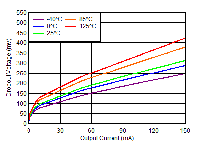
| VDO | Dropout voltage | Positive channel | IOUTP = 50 mA, 3.3 V ≤ VINP(nom) ≤ 33.0 V, VFBP = 1.070 V |
175 | 300 | mV | |
| IOUTP = 150 mA, 3.3 V ≤ VINP(nom) ≤ 33.0 V, VFBP = 1.070 V |
300 | 500 | |||||
| Negative channel | IOUTN = –50 mA, –3.3 V ≤ VINN(nom) ≤ –33.0 V, VFBN = 0.0695 V |
–250 | –145 | ||||
| IOUTN = –150 mA, –3.3 V ≤ VINN(nom) ≤ –33.0 V, VFBN = 0.0695 V |
–400 | –275 | |||||
| VBUF | Buffered reference output voltage | VNR/SS | V | ||||
| VBUF/IBUF | Buffered reference load regulation | IBUF = 100 µA to 1 mA | 1 | mV/mA | |||
| VBUF – VNR/SS | Output buffer offset voltage | VNR/SS = 0.25 V to 1.2 V | –4 | 3 | 8 | mV | |
| VOUTP–VOUTN | DC output voltage difference with a forced REF voltage | VNR/SS = 0.25 V to 1.2 V | –10 | 10 | %VNR/SS | ||
| ILIM | Current limit | Positive channel | VOUTP = 90% VOUTP(nom) | 200 | 330 | 500 | mA |
| Negative channel | VOUTN = 90% VOUTN(nom) | –500 | –300 | –200 | |||
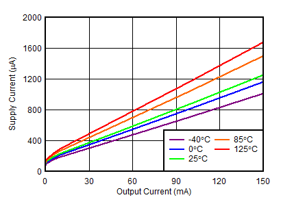
| ISUPPLY | Supply current | Positive channel | IOUTP = 0 mA, R2N = open, VINP = 33 V | 75 | 150 | µA | |
| IOUTP = 150 mA, R2N = open, VINP = 33 V | 904 | ||||||
| Negative channel | IOUTN = 0 mA, VOUTN(nom)= 0 V, R2N = open, VINN = –33 V | –150 | –60 | ||||
| IOUTN = 150 mA, R2N = open, VINN = –33 V | –1053 | ||||||
| ISHDN | Shutdown supply current | Positive channel | VEN = 0.4 V, VINP = 33 V | 3.75 | 6.5 | µA | |
| Negative channel | VEN = 0.4 V, VINN = –33 V | –4.5 | –2.25 | ||||
| IFBx | Feedback pin leakage current | Positive channel | 5.5 | 100 | nA | ||
| Negative channel | –100 | –9.7 | |||||
| INR/SS | Soft-start charging current | VNR/SS = 0.9 V | 3 | 5.1 | 6.7 | µA | |
| IEN | Enable pin leakage current | VEN = VINP = 33 V | 0.02 | 1 | µA | ||
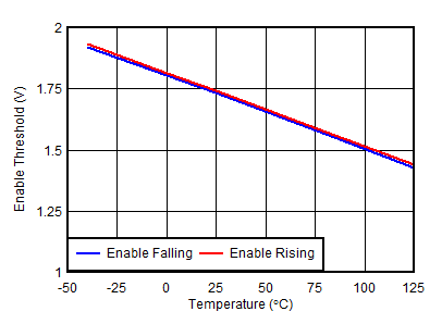
| VIH(EN) | Enable high-level voltage | 2.2 | VINP | V | |||
| VIL(EN) | Enable low-level voltage | 0 | 0.4 | V | |||
| PSRR | Power-supply rejection ratio | |VIN| = 6 V, |VOUT(nom)| = 5 V, COUT = 10 μF, CNR/SS = CFF= 10 nF, f = 120 Hz | 69 | dB | |||
| Vn | Output noise voltage | Positive channel | VINP = 3.3 V, VOUTP(nom) = VNR/SS, COUTP = 10 μF, CNR/SS = 10 nF, BW = 10 Hz to 100 kHz | 20.63 | µVRMS | ||
| VINP = 6 V, VOUTP(nom) = 5 V, COUTP = 10 μF, CNR/SS = CFF = 10 nF, BW = 10 Hz to 100 kHz | 26.86 | ||||||
| Negative channel | VINN = –3 V, VOUTN(nom) = –VNR/SS, COUTP = 10 μF, CNR/SS = 10 nF, BW = 10 Hz to 100 kHz | 22.13 | |||||
| VINN = –6 V, VOUTN(nom) = –5 V, COUTP = 10 μF, CNR/SS = CFF= 10 nF, BW = 10 Hz to 100 kHz | 28.68 | ||||||
| RNR/SS | Filter resistor from band gap to NR pin | 350 | kΩ | ||||
| Tsd | Thermal shutdown temperature | Shutdown, temperature increasing | 175 | °C | |||
| Reset, temperature decreasing | 160 | ||||||
(1) VOUT(target) = 0 V, R1N = 10 kΩ, R2N = open.
(2) To ensure VOUT does not drift up while the device is disabled, a minimum load current of 5 µA is required.
6.6 Startup Characteristics
at TJ = –40°C to +125°C, VINP(nom) = VOUTP(nom) + 1 V or VIN(nom) = 3.3 V (whichever is greater), VINN(nom) = VOUTN(nom) – 1 V or VINN(nom) = –3.3 V (whichever is less), VEN = VINP, IOUT = 1 mA, CINx = 2.2 μF, COUTx = 10 μF, CFFx = CNR/SS = 4.7nF, R1N = R2N = 10 kΩ, and FBP tied to OUTP (unless otherwise noted); typical values are at TJ = 25°C| PARAMETER | TEST CONDITIONS | MIN | TYP | MAX | UNIT | |
|---|---|---|---|---|---|---|
| tEN(delay) | Delay time from EN low-to-high transition to 2.5% VOUTP | From EN low-to-high transition to VOUTP = 2.5% × VOUTP(nom) | 300 | µs | ||
| tstart-up | Delay time from EN low-to-high transition to both outputs reaching 95% of final value | From EN low-to-high transition to VOUTP = VOUTP(nom) × 95% and VOUTN = VOUTN(nom) × 95% | 1.1 | ms | ||
| tPstart-Nstart | Delay time from VOUTP leaving a high-impedance state to VOUTN leaving a high-impedance state | From VOUTP = VOUTP(nom) × 2.5% to VOUTN = VOUTN(nom) × 2.5% | –40 | –17 | 40 | µs |
| Δ|VOUTP – VOUTN| | Voltage difference between the positive and negative output | During tPstart-Nstart | 75 | 300 | mV | |
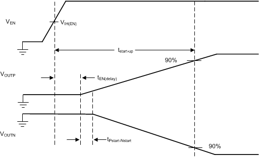
NOTE:
Slow ramps (trise(VINx) > 10 ms typically) on VINx with EN tied to VINP does not meet the tracking specification. Use a resistor divider from VINP to EN for these applications.6.7 Typical Characteristics
at TJ = 25°C, VINP = VOUTP(nom) + 1.0 V or VIN = 3.3 V (whichever is greater), VINN = VOUTN(nom) – 1 V or –3.3 V (whichever is less), VEN = VIN, IOUT = 1 mA, CIN = 10-μF ceramic, COUT = 10-μF ceramic, and CFFP = CFFN = CNR/SS = 10 nF (unless otherwise noted)
| VOUTP = 5 V, IOUTP = 150 mA, VOUTN = –5 V, IOUTN = 0 mA, CNR/SS = CFFx = 10 nF |
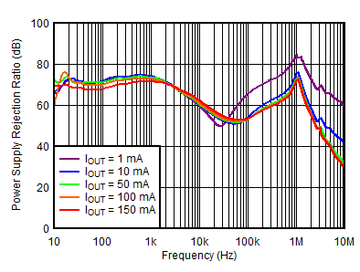
| VOUTP = 5 V, VINP = VEN = 6 V, VOUTN = –5 V, IOUTN = 0 mA, CNR/SS = CFFx = 10 nF |
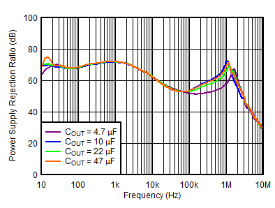
| VOUTP = 5 V, VINP = VEN = 6 V, VOUTN = –5 V, IOUTN = 0 mA, CNR/SS = CFFx = 10 nF |
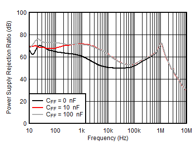
| VOUTP = 5 V, VINP = VEN = 6 V, VOUTN = –5 V, IOUTN = 0 mA, CNR/SS = 10 nF |
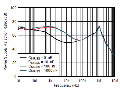
| VOUTP = 5 V, VINP = VEN = 6 V, VOUTN = –5 V, IOUTN = 0 mA, CFFx = 10 nF |
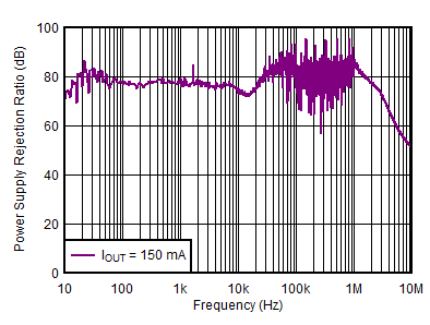
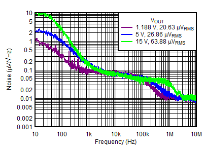
| IOUTP = 150 mA, VINP = VEN, VOUTN = –VOUTP, IOUTN = 0 mA, CNR/SS = CFFx = 10 nF |
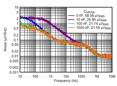
| VOUTP = 5 V, IOUTP = 150 mA, VINP = VEN = 6 V, VOUTN = –5 V, IOUTN = 0 mA, CFFx = 10 nF |
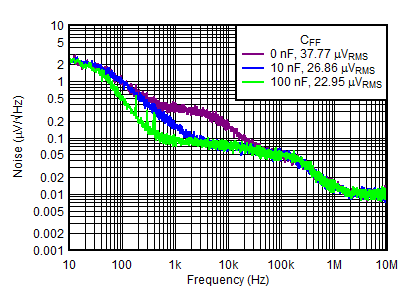
| VOUTP = 5 V, IOUTP = 150 mA, VINP = VEN = 6 V, VOUTN = –5 V, IOUTN = 0 mA, CNR/SS = 10 nF |
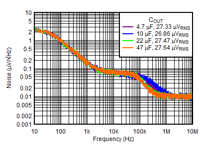
| VOUTP = 5 V, IOUTP = 150 mA, VINP = VEN = 6 V, VOUTN = –5 V, IOUTN = 0 mA, CNR/SS = CFFx = 10 nF |
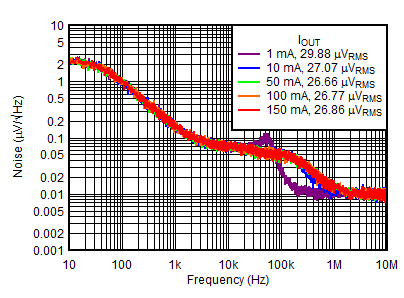
| VOUTP = 5 V, VINP = VEN = 6 V, VOUTN = –5 V, IOUTN = 0 mA, CNR/SS = CFFx = 10 nF |
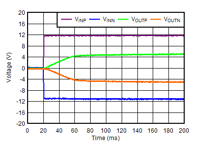
| VOUTP = –VOUTN = 5 V, VINP = –VINN = 12 V |
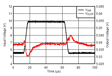
| VINP = 5.5 V to 10 V at 1 V/µs, VOUTP = –VOUTN = 5 V, IOUTN = 0 mA, IOUTP = 150 mA |
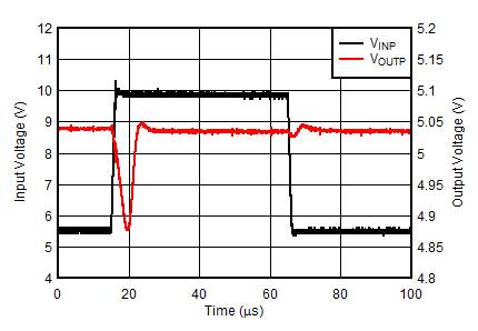
| VINP = 5.5 V to 10 V at 4 V/µs, VOUTP = –VOUTN = 5 V, IOUTN = 0 mA, IOUTP = 150 mA |
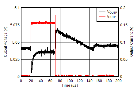
| VINP = 6 V, VOUTP = –VOUTN = 5 V, IOUTN = 0 mA, IOUTP = 1 mA to 150 mA at 1 A/µs |
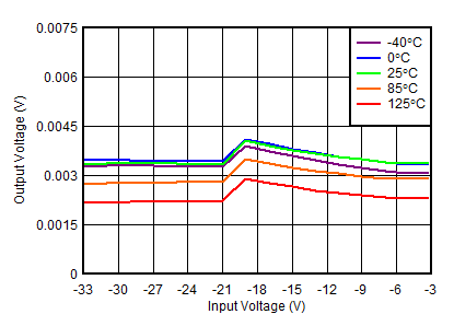
| VOUTN = 0 V |
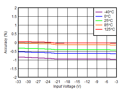
| VOUTN = –1.19 V |
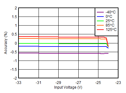
| VOUTN = –24 V |
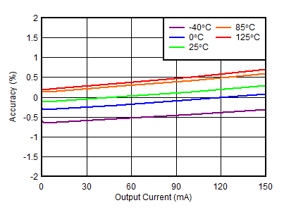
| VOUTN = –15 V, VINN = –16 V |
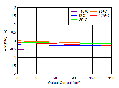
| VOUTP = 1.188 V, VINP = 3.3 V |
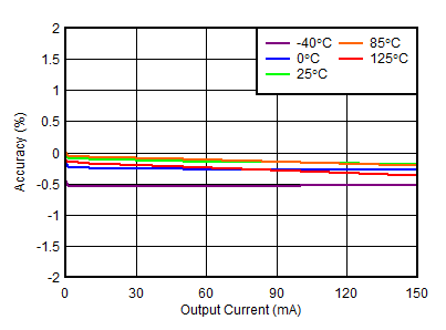
| VOUTP = 30 V, VINP = 33 V |
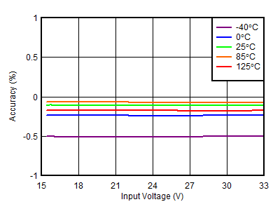
| VOUTP = 15 V |
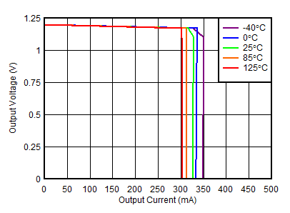
| VOUTP = 1.188 V |
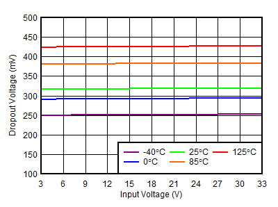
Input Voltage
| VINP = 3.3 V |
Output Current
Output Voltage
| VOUTP = 1.188 V |
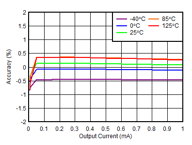
| VOUTN = –1.19 V |
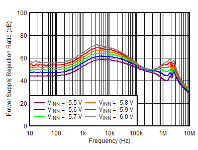
| VOUTP = 5 V, IOUTP = 0 mA, VOUTN = –5 V, IOUTN = 150 mA, CNR/SS = CFFx = 10 nF |
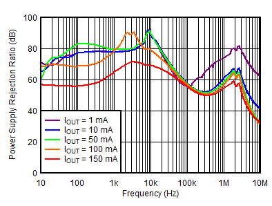
| VOUTP = 5 V, IOUTP = 0 mA, VINN = –6 V, VOUTN = –5 V, CNR/SS = CFFx = 10 nF |
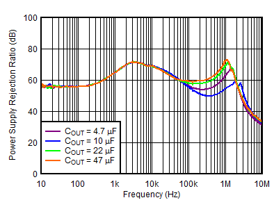
| VOUTP = 5 V, IOUTP = 0 mA, VINN = –6 V, VOUTN = –5 V, CNR/SS = CFFx = 10 nF, COUTP = 10 µF |
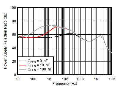
| VOUTP = 5 V, IOUTP = 0 mA, VINN = –6 V, VOUTN = –5 V, CNR/SS = CFFP = 10 nF |
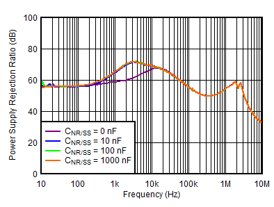
| VOUTP = 5 V, IOUTP = 0 mA, VINN = –6 V, VOUTN = –5 V, CFFx = 10 nF |
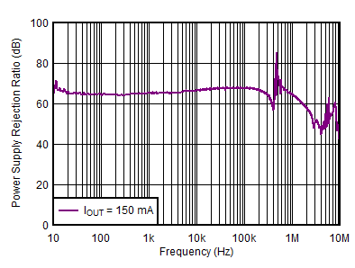
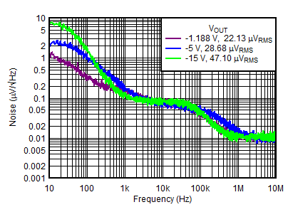
| IOUTN = –150 mA, VINP = VEN, VOUTN = –VOUTP, IOUTP = 0 mA, CNR/SS = CFFx = 10 nF |
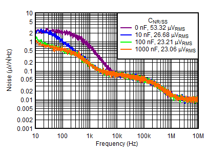
| VOUTN = –5 V, IOUTN = –150 mA, VINP = VEN = 6 V, VOUTN = –5 V, IOUTP = 0 mA, CFFx = 10 nF |
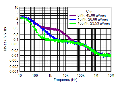
| VOUTN = –5 V, IOUTN = –150 mA, VINP = VEN = 6 V, VOUTN = –5 V, IOUTP = 0 mA, CNR/SS = 10 nF |

| VOUTN = –5 V, IOUTN = –150 mA, VINP = VEN = 6 V, VOUTN = –5 V, IOUTP = 0 mA, CNR/SS = CFFx = 10 nF |
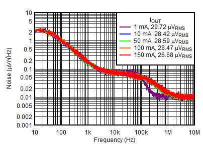
| VOUTN = –5 V, VINP = VEN = 6 V, VOUTN = –5 V, IOUTP = 0 mA, CNR/SS = CFFx = 10 nF |
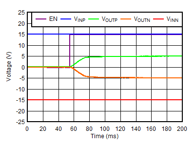
| VOUTP = –VOUTN = 5 V, VINP = –VINN = 15 V |
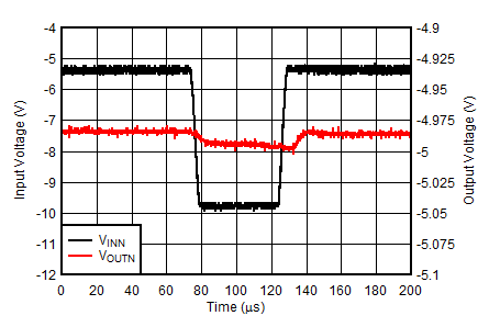
| VINN = –5.5 V to –10 V at 1 V/µs, VOUTP = –VOUTN = 5 V, IOUTN = –150 mA, IOUTP = 0 mA |
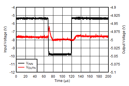
| VINN = –5.5 V to –10 V at 4 V/µs, VOUTP = –VOUTN = 5 V, IOUTN = –150 mA, IOUTP = 0 mA |
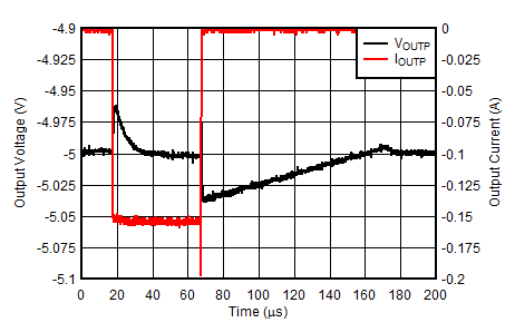
| VINN = –6 V, VOUTP = –VOUTN = 5 V, IOUTN = 0 mA, IOUTN = –1 mA to –150 mA at 1 A/µs |
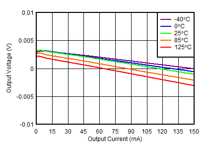
| VOUTN = 0 V, VINN = –3.3 V |
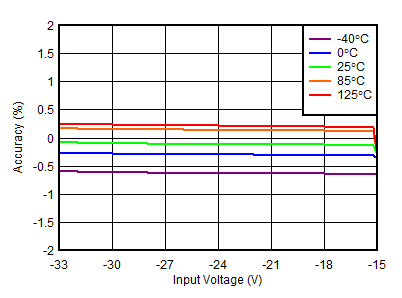
| VOUTN = –15 V |
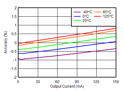
| VOUTN = –1.2 V, VINN = –3.3 V |
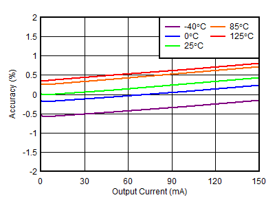
| VOUTN = –30 V, VINN = –33 V |
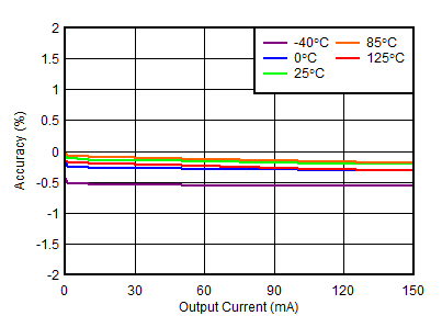
| VOUTP = 15 V, VINP = 16 V |
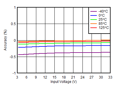
| VOUTP = 1.188 V |
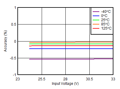
| VOUTP = 24 V |
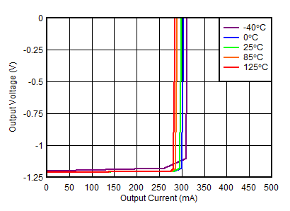
| VOUTN = –1.19 V |
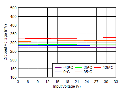
Input Voltage
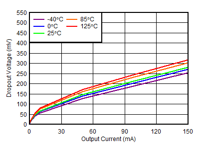
| VOUTN = –3.3 V |
Output Current
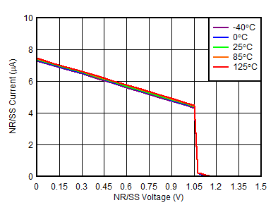
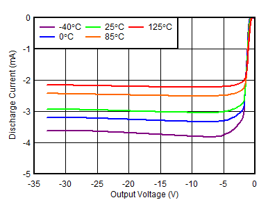
Output Voltage
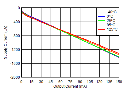
| VOUTN = –1.19 V |