ZHCS120B March 2011 – July 2015 TPS7A4001
PRODUCTION DATA.
6 Specifications
6.1 Absolute Maximum Ratings
over operating junction temperature range (unless otherwise noted)(1)| MIN | MAX | UNIT | ||
|---|---|---|---|---|
| Voltage | IN pin to GND pin | –0.3 | 105 | V |
| OUT pin to GND pin | –0.3 | 105 | ||
| OUT pin to IN pin | –105 | 0.3 | ||
| FB pin to GND pin | –0.3 | 2 | ||
| FB pin to IN pin | –105 | 0.3 | ||
| EN pin to IN pin | –105 | 0.3 | ||
| EN pin to GND pin | –0.3 | 105 | ||
| Current | Peak output | Internally limited | ||
| Temperature | Operating virtual junction, TJ | –40 | 125 | °C |
| Storage, Tstg | –65 | 150 | ||
(1) Stresses beyond those listed under Absolute Maximum Ratings may cause permanent damage to the device. These are stress ratings only, which do not imply functional operation of the device at these or any other conditions beyond those indicated under Recommended Operating Conditions. Exposure to absolute-maximum-rated conditions for extended periods may affect device reliability.
6.2 ESD Ratings
| VALUE | UNIT | |||
|---|---|---|---|---|
| V(ESD) | Electrostatic discharge | Human-body model (HBM), per ANSI/ESDA/JEDEC JS-001(1) | ±2500 | V |
| Charged-device model (CDM), per JEDEC specification JESD22-C101(2) | ±500 | |||
(1) JEDEC document JEP155 states that 500-V HBM allows safe manufacturing with a standard ESD control process.
(2) JEDEC document JEP157 states that 250-V CDM allows safe manufacturing with a standard ESD control process.
6.3 Recommended Operating Conditions
over operating junction temperature range (unless otherwise noted)| MIN | NOM | MAX | UNIT | ||
|---|---|---|---|---|---|
| VIN | 7 | 100 | V | ||
| VOUT | 1.161 | 90 | V | ||
| VEN | 0 | 100 | V | ||
| IOUT | 0 | 50 | mA | ||
6.4 Thermal Information
| THERMAL METRIC(1) | TPS7A4001 | UNIT | |
|---|---|---|---|
| DGN (HVVSOP) | |||
| 8 PINS | |||
| RθJA | Junction-to-ambient thermal resistance | 66.7 | °C/W |
| RθJC(top) | Junction-to-case (top) thermal resistance | 54.1 | °C/W |
| RθJB | Junction-to-board thermal resistance | 38.1 | °C/W |
| ψJT | Junction-to-top characterization parameter | 2 | °C/W |
| ψJB | Junction-to-board characterization parameter | 37.8 | °C/W |
| RθJC(bot) | Junction-to-case (bottom) thermal resistance | 15.5 | °C/W |
(1) For more information about traditional and new thermal metrics, see the Semiconductor and IC Package Thermal Metrics application report, SPRA953.
6.5 Electrical Characteristics
At TJ = –40°C to 125°C, VIN = VOUT(NOM) + 2 V or VIN = 7 V (whichever is greater), VEN = VIN, IOUT = 100 µA, CIN = 1 μF, COUT = 4.7 μF, and FB tied to OUT, unless otherwise noted.| PARAMETER | TEST CONDITIONS | MIN | TYP | MAX | UNIT | |||
|---|---|---|---|---|---|---|---|---|
| VIN | Input voltage | 7 | 100 | V | ||||
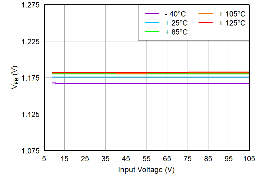
| VREF | Internal reference | TJ = 25°C, VFB = VREF, VIN = 9 V, IOUT = 25 mA | 1.161 | 1.173 | 1.185 | V | ||
| VOUT | Output voltage range(1) | VIN ≥ VOUT(NOM) + 2 V | VREF | 90 | V | |||
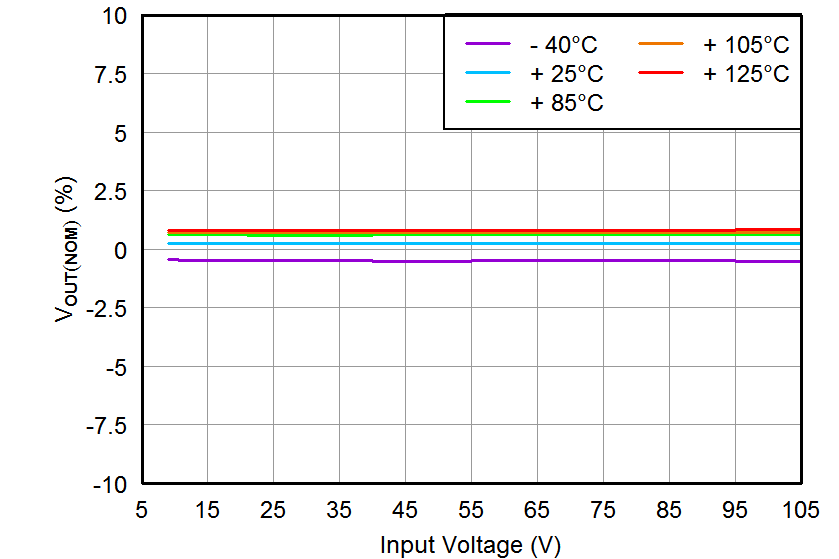
| Nominal accuracy | TJ = 25°C, VIN = 9 V, IOUT = 25 mA | –1 | 1 | %VOUT | ||||
| Overall accuracy | VOUT(NOM) + 2 V ≤ VIN ≤ 24 V(2)
100 µA ≤ IOUT ≤ 50 mA |
–2.5 | 2.5 | %VOUT | ||||
 |
Line regulation | 7 V ≤ VIN ≤ 100 V | 0.03 | %VOUT | ||||
 |
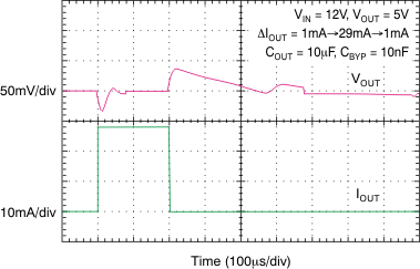
Load regulation | 100 µA ≤ IOUT ≤ 50 mA | 0.31 | %VOUT | ||||
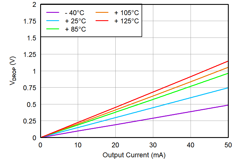
| VDO | Dropout voltage | VIN = 17 V, VOUT(NOM) = 18 V, IOUT = 20 mA | 290 | mV | ||||
| VIN = 17 V, VOUT(NOM) = 18 V, IOUT = 50mA | 0.78 | 1.3 | V | |||||
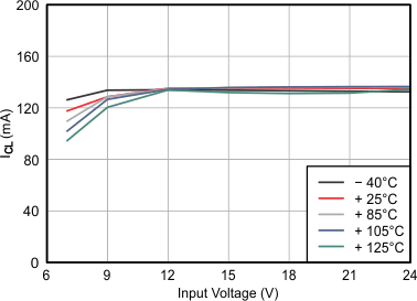
| ILIM | Current limit | VOUT = 90% VOUT(NOM), VIN = 7 V, TJ ≤ 85°C | 51 | 117 | 200 | mA | ||
| VOUT = 90% VOUT(NOM), VIN = 9 V | 51 | 128 | 200 | mA | ||||
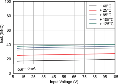
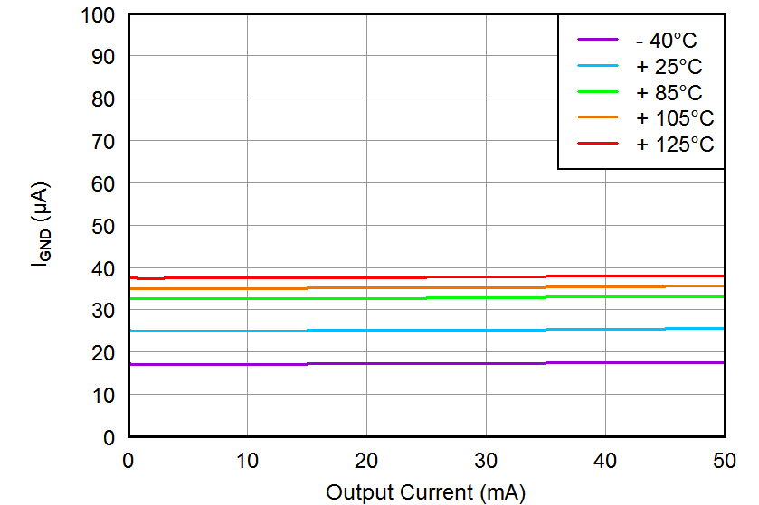
| IGND | Ground current | 7 V ≤ VIN ≤ 100 V, IOUT = 0 mA | 25 | 65 | μA | |||
| IOUT = 50 mA | 25 | μA | ||||||
| ISHDN | Shutdown supply current | VEN = 0.4 V | 4.1 | 20 | μA | |||
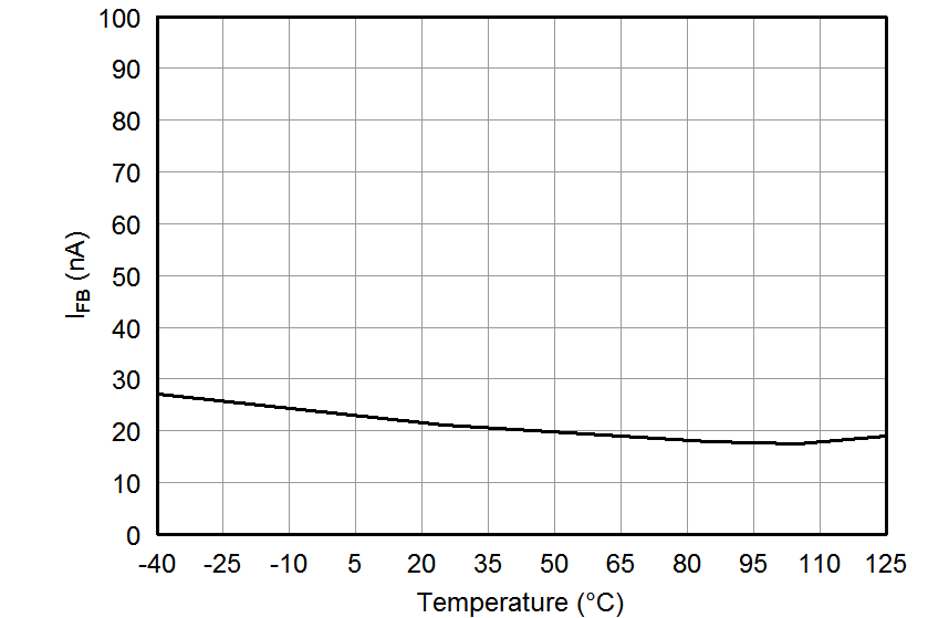
| IFB | Feedback current(3) | –0.1 | 0.01 | 0.1 | µA | |||
| IEN | Enable current | 7 V ≤ VIN ≤ 100 V, VIN = VEN | 0.02 | 1 | μA | |||
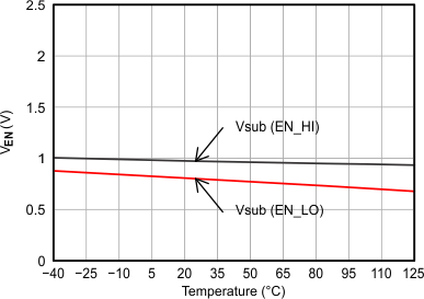
| VEN_HI | Enable high-level voltage | 1.5 | VIN | V | ||||
| VEN_LO | Enable low- level voltage | 0 | 0.4 | V | ||||
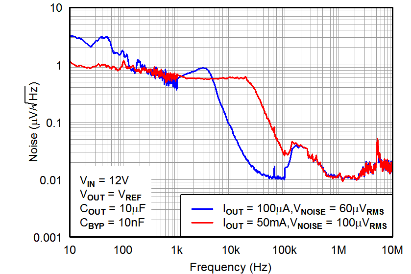
| VNOISE | Output noise voltage | VIN = 12 V, VOUT(NOM) = VREF, COUT = 10 μF, BW = 10 Hz to 100 kHz |
58 | μVRMS | ||||
| VIN = 12 V, VOUT(NOM) = 5 V, COUT = 10 μF, CBYP(4) = 10 nF, BW = 10 Hz to 100 kHz | 73 | μVRMS | ||||||
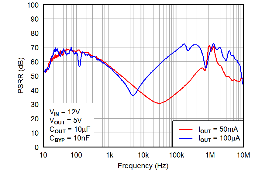
| PSRR | Power-supply rejection ratio | VIN = 12 V, VOUT(NOM) = 5 V, COUT = 10 μF, CBYP(4) = 10 nF, ƒ = 100 Hz | 65 | dB | ||||
| TSD | Thermal shutdown temperature | Shutdown, temperature increasing | 170 | °C | ||||
| Reset, temperature decreasing | 150 | °C | ||||||
| TJ | Operating junction temperature | –40 | 125 | °C | ||||
(1) To ensure stability at no-load conditions, a current from the feedback resistive network greater than or equal to 10μA is required.
(2) Maximum input voltage is limited to 24 V because of the package power dissipation limitations at full load (P ≈ (VIN – VOUT) × IOUT = (24 V – VREF) × 50 mA ≈ 1.14 W). The device is capable of sourcing a maximum current of 50 mA at higher input voltages as long as the power dissipated is within the thermal limits of the package plus any external heatsinking.
(3) IFB > 0 flows out of the device.
(4) CBYP refers to a bypass capacitor connected to the FB and OUT pins.
6.6 Typical Characteristics
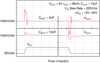
At TJ = –40°C to 125°C, VIN = VOUT(NOM) + 2 V or VIN = 9 V (whichever is greater), VEN = VIN, IOUT = 100 µA, CIN = 1 μF, COUT = 4.7 μF, and FB tied to OUT, unless otherwise noted.