ZHCS515A December 2011 – August 2015 TPS7A4201
PRODUCTION DATA.
6 Specifications
6.1 Absolute Maximum Ratings
over operating free-air temperature range (unless otherwise noted).(1)| MIN | MAX | UNIT | ||
|---|---|---|---|---|
| Voltage | IN pin to GND pin | –0.3 | +30 | V |
| OUT pin to GND pin | –0.3 | +30 | V | |
| OUT pin to IN pin | –30 | +0.3 | V | |
| FB pin to GND pin | –0.3 | +2 | V | |
| FB pin to IN pin | –30 | +0.3 | V | |
| EN pin to IN pin | –30 | 0.3 | V | |
| EN pin to GND pin | –0.3 | +30 | V | |
| Current | Peak output | Internally limited | ||
| Temperature | Operating junction temperature, TJ | –40 | +125 | °C |
| Storage, Tstg | –65 | +150 | °C | |
(1) Stresses beyond those listed under Absolute Maximum Ratings may cause permanent damage to the device. These are stress ratings only, and functional operation of the device at these or any other conditions beyond those indicated is not implied. Exposure to absolute-maximum rated conditions for extended periods may affect device reliability.
6.2 ESD Ratings
| VALUE | UNIT | |||
|---|---|---|---|---|
| V(ESD) | Electrostatic discharge | Human body model (HBM), per ANSI/ESDA/JEDEC JS-001(1) | ±2500 | V |
| Charged-device model (CDM), per JEDEC specification JESD22-C101(2) | ±500 | |||
(1) JEDEC document JEP155 states that 500-V HBM allows safe manufacturing with a standard ESD control process.
(2) JEDEC document JEP157 states that 250-V CDM allows safe manufacturing with a standard ESD control process.
6.3 Recommended Operating Conditions
over operating junction temperature range (unless otherwise noted)| MIN | NOM | MAX | UNIT | ||
|---|---|---|---|---|---|
| VIN | 7 | 28 | V | ||
| VOUT | 1.161 | 26 | V | ||
| VEN | 0 | 28 | V | ||
| IOUT | 0 | 50 | mA | ||
6.4 Thermal Information
| THERMAL METRIC(1) | TPS7A4201 | UNIT | |
|---|---|---|---|
| DGN (MSOP) | |||
| 8 PINS | |||
| RθJA | Junction-to-ambient thermal resistance | 66.7 | °C/W |
| RθJC(top) | Junction-to-case (top) thermal resistance | 54.1 | °C/W |
| RθJB | Junction-to-board thermal resistance | 38.1 | °C/W |
| ψJT | Junction-to-top characterization parameter | 2.0 | °C/W |
| ψJB | Junction-to-board characterization parameter | 37.8 | °C/W |
| RθJC(bot) | Junction-to-case (bottom) thermal resistance | 15.5 | °C/W |
(1) For more information about traditional and new thermal metrics, see the Semiconductor and IC Package Thermal Metrics application report, SPRA953.
6.5 Electrical Characteristics
At TJ = –40°C to +125°C, VIN = VOUT(NOM) + 2.0 V or VIN = 7.0 V (whichever is greater), VEN = VIN, IOUT = 100 µA, CIN = 1 μF, COUT = 4.7 μF, and FB tied to OUT, unless otherwise noted.| PARAMETER | TEST CONDITIONS | MIN | TYP | MAX | UNIT | |||
|---|---|---|---|---|---|---|---|---|
| VIN | Input voltage range | 7.0 | 28.0 | V | ||||
| VREF | Internal reference | TJ = +25°C, VFB = VREF, VIN = 9 V, IOUT = 25 mA | 1.161 | 1.173 | 1.185 | V | ||
| VOUT | Output voltage range(1) | VIN ≥ VOUT(NOM) + 2.0 V | VREF | 26 | V | |||
| Nominal accuracy | TJ = +25°C, VIN = 9 V, IOUT = 25 mA | –1.0 | +1.0 | %VOUT | ||||
| Overall accuracy | VOUT(NOM) + 2.0 V ≤ VIN ≤ 24 V(2)
100 µA ≤ IOUT ≤ 50 mA |
–2.5 | +2.5 | %VOUT | ||||
| ΔVO(ΔVI) | Line regulation | 7 V ≤ VIN ≤ 28 V | 0.03 | %VOUT | ||||
| ΔVO(ΔVL) | Load regulation | 100 µA ≤ IOUT ≤ 50 mA | 0.31 | %VOUT | ||||
| VDO | Dropout voltage | VIN = 17 V, VOUT(NOM) = 18 V, IOUT = 20 mA | 290 | mV | ||||
| VIN = 17 V, VOUT(NOM) = 18 V, IOUT = 50 mA | 0.78 | 1.3 | V | |||||
| ILIM | Current limit | VOUT = 90% VOUT(NOM), VIN = 7.0 V, TJ ≤ +85°C | 65 | 117 | 200 | mA | ||
| VOUT = 90% VOUT(NOM), VIN = 9.0 V | 65 | 128 | 200 | mA | ||||
| IGND | Ground current | 7 V ≤ VIN ≤ 28 V, IOUT = 0 mA | 25 | 65 | μA | |||
| IOUT = 50 mA | 25 | μA | ||||||
| ISHDN | Shutdown supply current | VEN = +0.4 V | 4.1 | 20 | μA | |||
| I FB | Feedback current(3) | –0.1 | 0.01 | 0.1 | µA | |||
| IEN | Enable current | 7 V ≤ VIN ≤ 28 V, VIN = VEN | 0.02 | 1.0 | μA | |||
| VEN_HI | Enable high-level voltage | 1.5 | VIN | V | ||||
| VEN_LO | Enable low- level voltage | 0 | 0.4 | V | ||||
| VNOISE | Output noise voltage | VIN = 12 V, VOUT(NOM) = VREF, COUT = 10 μF, BW = 10 Hz to 100 kHz |
58 | μVRMS | ||||
| VIN = 12 V, VOUT(NOM) = 5 V, COUT = 10 μF, CBYP(4) = 10 nF, BW = 10 Hz to 100 kHz | 73 | μVRMS | ||||||
| PSRR | Power-supply rejection ratio | VIN = 12 V, VOUT(NOM) = 5 V, COUT = 10 μF, CBYP(4) = 10 nF, f = 100 Hz | 65 | dB | ||||
| TSD | Thermal shutdown temperature | Shutdown, temperature increasing | +170 | °C | ||||
| Reset, temperature decreasing | +150 | °C | ||||||
| TJ | Operating junction temperature range | –40 | +125 | °C | ||||
(1) To ensure stability at no-load conditions, a current from the feedback resistive network greater than or equal to 10 μA is required.
(2) Maximum input voltage (VIN) is limited to 24 V because of the package power dissipation limitations at full load [P ≈ (VIN – VOUT) × IOUT = (24 V – VREF) × 50 mA ≈ 1.14 V], given an ambient temperature of +50°C. The device is capable of sourcing steady-state load currents as high as 60 mA at higher input voltages without damage if the maximum operating junction temperature (TJ) is not exceeded. The Electrical Characteristics are not characterized for load current (IOUT) exceeding 50 mA.
(3) IFB > 0 flows out of the device.
(4) CBYP refers to a bypass capacitor connected to the FB and OUT pins.
6.6 Dissipation Ratings
| BOARD | PACKAGE | RθJA | RθJC | DERATING FACTOR ABOVE TA = +25°C | TA ≤ +25°C POWER RATING | TA = +70°C POWER RATING | TA = +85°C POWER RATING |
|---|---|---|---|---|---|---|---|
| High-K(1) | DGN | 55.9°C/W | 8.47°C/W | 16.6mW/°C | 1.83W | 1.08W | 0.833W |
(1) The JEDEC High-K (2s2p) board design used to derive this data was a 3-inch x 3-inch multilayer board with 2-ounce internal power and ground planes and 2-ounce copper traces on top and bottom of the board.
6.7 Typical Characteristics
At TJ = –40°C to +125°C, VIN = VOUT(NOM) + 2.0 V or VIN = 9.0 V (whichever is greater), VEN = VIN, IOUT = 100 µA, CIN = 1 μF, COUT = 4.7 μF, and FB tied to OUT, unless otherwise noted.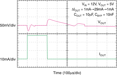 Figure 1. Load Transient Response
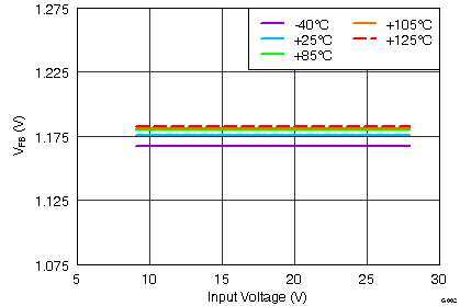 Figure 3. Feedback Voltage
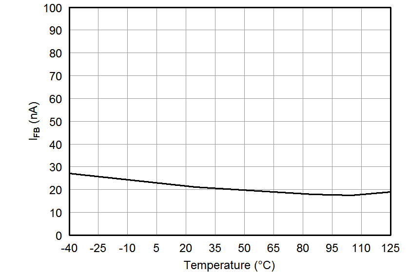 Figure 5. Feedback Current
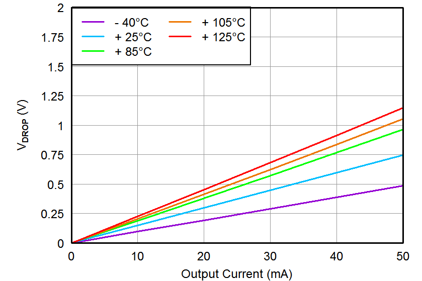 Figure 7. Dropout Voltage
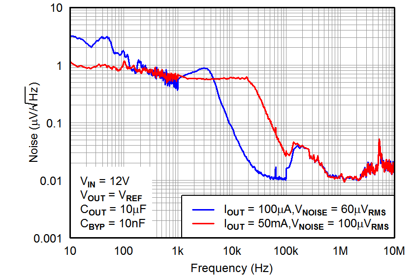 Figure 9. Output Spectral Noise Density
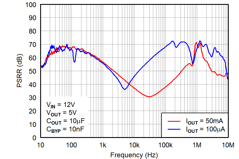 Figure 11. Power-Supply Rejection Ratio
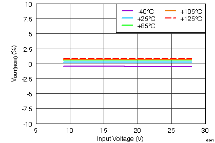 Figure 2. Line Regulation
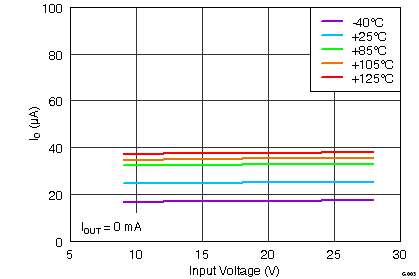 Figure 4. Quiescent Current vs Input Voltage
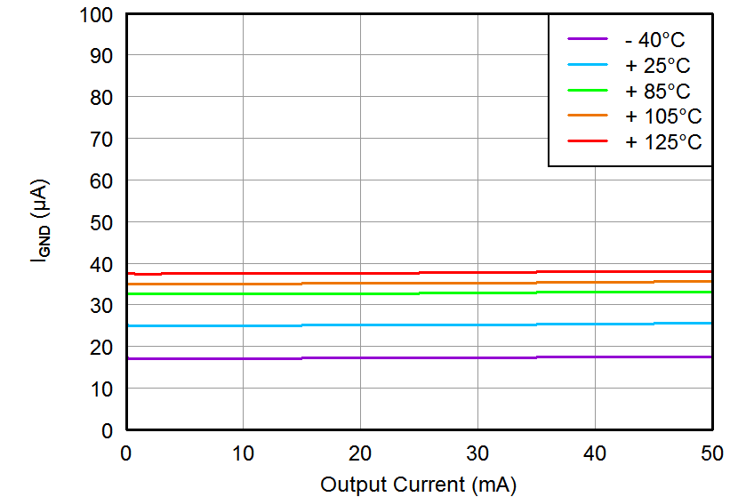 Figure 6. Ground Current
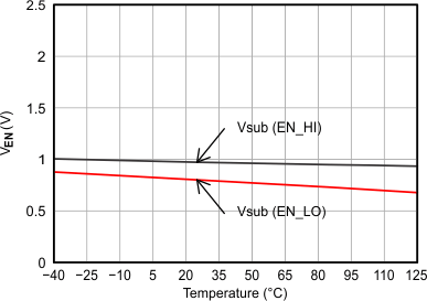 Figure 8. Enable Threshold Voltage
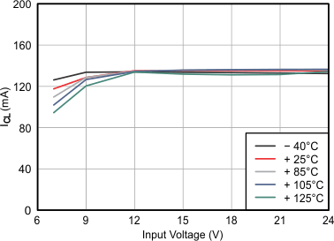 Figure 10. Current Limit