ZHCS515A December 2011 – August 2015 TPS7A4201
PRODUCTION DATA.
7 Detailed Description
7.1 Overview
The TPS7A4201 belongs to a new generation of linear regulators that use an innovative BiCMOS process technology to achieve very high maximum input and output voltages.
This process not only allows the TPS7A4201 to maintain regulation during very fast voltage transients up to 28 V, but it also allows the TPS7A4201 to regulate from a continuous high-voltage input rail. Unlike other regulators created using bipolar technology, the TPS7A4201 ground current is also constant over its output current range, resulting in increased efficiency and lower power consumption.
These features, combined with a high thermal performance MSOP-8 PowerPAD package, make this device ideal for industrial and telecom applications.
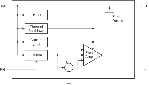
7.2 Functional Block Diagram

7.3 Feature Description
7.3.1 Enable Pin Operation
The TPS7A4201 provides an enable pin (EN) feature that turns on the regulator when VEN > 1.5 V.
7.3.2 Thermal Protection
Thermal protection disables the output when the junction temperature rises to approximately 170°C, allowing the device to cool. When the junction temperature cools to approximately 150°C, the output circuitry is enabled. Depending on power dissipation, thermal resistance, and ambient temperature, the thermal protection circuit may cycle on and off. This cycling limits the dissipation of the regulator, protecting it from damage as a result of overheating.
Any tendency to activate the thermal protection circuit indicates excessive power dissipation or an inadequate heatsink. For reliable operation, limit junction temperature to a maximum of 125°C. To estimate the margin of safety in a complete design (including heatsink), increase the ambient temperature until the thermal protection is triggered; use worst-case loads and signal conditions. For good reliability, trigger thermal protection at least 35°C above the maximum expected ambient condition of your particular application. This configuration produces a worst-case junction temperature of 125°C at the highest expected ambient temperature and worst-case load.
The internal protection circuitry of the TPS7A4201 device has been designed to protect against overload conditions. The protection circuitry was not intended to replace proper heatsinking. Continuously running the TPS7A4201 device into thermal shutdown degrades device reliability.
7.4 Device Functional Modes
7.4.1 Normal Operation
The device regulates to the nominal output voltage under the following conditions:
- The input voltage is at least as high as VIN(min).
- The input voltage is greater than the nominal output voltage added to the dropout voltage.
- The enable voltage has previously exceeded the enable rising threshold voltage and has not decreased below the enable falling threshold.
- The output current is less than the current limit.
- The device junction temperature is less than the maximum specified junction temperature.
7.4.2 Dropout Operation
If the input voltage is lower than the nominal output voltage plus the specified dropout voltage, but all other conditions are met for normal operation, the device operates in dropout mode. In this mode of operation, the output voltage is the same as the input voltage minus the dropout voltage. The transient performance of the device is significantly degraded because the pass device (as a bipolar junction transistor, or BJT) is in saturation and no longer controls the current through the LDO. Line or load transients in dropout can result in large output voltage deviations.
7.4.3 Disabled
The device is disabled under the following conditions:
- The enable voltage is less than the enable falling threshold voltage or has not yet exceeded the enable rising threshold.
- The device junction temperature is greater than the thermal shutdown temperature.
Table 1 lists the conditions that lead to the different modes of operation.