ZHCSME0B December   2020  – November 2022 TPS7A43

PRODUCTION DATA  

  1. 特性
  2. 应用
  3. 说明
  4. Revision History
  5. Pin Configuration and Functions
  6. Specifications
    1. 6.1 Absolute Maximum Ratings
    2. 6.2 ESD Ratings
    3. 6.3 Recommended Operating Conditions
    4. 6.4 Thermal Information
    5. 6.5 Electrical Characteristics
    6. 6.6 Typical Characteristics
  7. Detailed Description
    1. 7.1 Overview
    2. 7.2 Functional Block Diagrams
    3. 7.3 Feature Description
      1. 7.3.1 MID_OUT Voltage Selection
      2. 7.3.2 Precision Enable
      3. 7.3.3 Dropout Voltage
      4. 7.3.4 Current Limit
      5. 7.3.5 Thermal Shutdown
      6. 7.3.6 Power Good
    4. 7.4 Device Functional Modes
      1. 7.4.1 Device Functional Mode Comparison
      2. 7.4.2 Normal Operation
      3. 7.4.3 Dropout Operation
      4. 7.4.4 Disabled
  8. Application and Implementation
    1. 8.1 Application Information
      1. 8.1.1 MID_OUT Voltage Setting
      2. 8.1.2 Adjustable Device Feedback Resistors
      3. 8.1.3 Recommended Capacitor Types
      4. 8.1.4 Input and Output Capacitor Requirements
      5. 8.1.5 Power Dissipation (PD)
      6. 8.1.6 Estimating Junction Temperature
    2. 8.2 Typical Application
      1. 8.2.1 Design Requirements
      2. 8.2.2 Detailed Design Procedure
      3. 8.2.3 Application Curves
    3. 8.3 Power Supply Recommendations
    4. 8.4 Layout
      1. 8.4.1 Layout Guidelines
      2. 8.4.2 Layout Examples
  9. Device and Documentation Support
    1. 9.1 Device Support
      1. 9.1.1 Development Support
        1. 9.1.1.1 Evaluation Modules
        2. 9.1.1.2 Spice Models
      2. 9.1.2 Device Nomenclature
    2. 9.2 Documentation Support
      1. 9.2.1 Related Documentation
    3. 9.3 接收文档更新通知
    4. 9.4 支持资源
    5. 9.5 Trademarks
    6. 9.6 Electrostatic Discharge Caution
    7. 9.7 术语表
  10. 10Mechanical, Packaging, and Orderable Information

封装选项

机械数据 (封装 | 引脚)
散热焊盘机械数据 (封装 | 引脚)
订购信息

Precision Enable

The TPS7A43 features a precision enable circuit. The enable pin (EN) is active high; thus, enable the device by forcing the voltage of the enable pin to exceed the VEN(HI) voltage; see the Section 6.5 table. Turn off the device by forcing the voltage of the enable pin to drop below the VEN(LOW) voltage; see the Section 6.5 table. EN is pulled high by a 50-nA current source; therefore, EN can be left floating to enable the device. Board-level leakage on the order of tens of nanoamperes can cause the EN pin to be pulled low when EN is left floating, so care must be taken to minimize leakage if this functionality is used.

If this pin is tied to the IN pin, the input voltage must not exceed 18 V; see the Section 6.3 table.

As shown in Figure 7-3, an external resistor divider circuit can be used to enable the device using the input voltage.
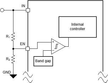
GUID-20210908-SS0I-6FDP-MQ3P-NXKF2VQXF02M-low.gif Figure 7-3 Enable the Device Using the Input Voltage

The VEN(HI) (maximum) and VEN(LOW) (minimum) thresholds along with the application input voltage can be used to set the R1 to R2 resistor divider ratio. The values of the R2 and R1 resistors can also be optimized to minimize the leakage current through the divider.