ZHCS992F June   2012  – September 2014

PRODUCTION DATA.  

  1. 特性
  2. 应用
  3. 说明
  4. 修订历史记录
  5. Pin Configuration and Functions
  6. Specifications
    1. 6.1 Absolute Maximum Ratings
    2. 6.2 Handling Ratings
    3. 6.3 Recommended Operating Conditions
    4. 6.4 Thermal Information
    5. 6.5 Electrical Characteristics
    6. 6.6 Typical Characteristics
  7. Detailed Description
    1. 7.1 Overview
    2. 7.2 Functional Block Diagram
    3. 7.3 Feature Description
      1. 7.3.1 Internal Current Limit (ICL)
      2. 7.3.2 Enable (EN) And Under-Voltage Lockout (UVLO)
      3. 7.3.3 Soft-Start And Inrush Current
    4. 7.4 Device Functional Modes
    5. 7.5 Programming
      1. 7.5.1 ANY-OUT Programmable Output Voltage
      2. 7.5.2 Adjustable Operation (TPS7A4701 Only)
  8. Application and Implementation
    1. 8.1 Application Information
    2. 8.2 Typical Application
      1. 8.2.1 Design Requirements
      2. 8.2.2 Detailed Design Procedure
        1. 8.2.2.1 Capacitor Recommendations
          1. 8.2.2.1.1 Input and Output Capacitor Requirements
          2. 8.2.2.1.2 Noise Reduction Capacitor (CNR)
        2. 8.2.2.2 Dropout Voltage (VDO)
        3. 8.2.2.3 Output Voltage Accuracy
        4. 8.2.2.4 Startup
        5. 8.2.2.5 AC Performance
          1. 8.2.2.5.1 Power-Supply Rejection Ratio (PSRR)
          2. 8.2.2.5.2 Load Step Transient Response
          3. 8.2.2.5.3 Noise
      3. 8.2.3 Application Curves
  9. Power Supply Recommendations
    1. 9.1 Power Dissipation (PD)
  10. 10Layout
    1. 10.1 Layout Guidelines
    2. 10.2 Layout Example
    3. 10.3 Thermal Protection
    4. 10.4 Estimating Junction Temperature
  11. 11器件和文档支持
    1. 11.1 文档支持
      1. 11.1.1 相关文档 
    2. 11.2 相关链接
    3. 11.3 商标
    4. 11.4 静电放电警告
    5. 11.5 术语表
  12. 12机械封装和可订购信息

封装选项

机械数据 (封装 | 引脚)
散热焊盘机械数据 (封装 | 引脚)
订购信息

6 Specifications

6.1 Absolute Maximum Ratings

Over junction temperature range, unless otherwise noted.(1)
MIN MAX UNIT
Voltage(2) IN pin to GND pin –0.4 +36 V
EN pin to GND pin –0.4 +36 V
EN pin to IN pin –36 +0.4 V
OUT pin to GND pin –0.4 +36 V
NR pin to GND pin –0.4 +36 V
SENSE/FB pin to GND pin –0.4 +36 V
0P1V pin to GND pin –0.4 +36 V
0P2V pin to GND pin –0.4 +36 V
0P4V pin to GND pin –0.4 +36 V
0P8V pin to GND pin –0.4 +36 V
1P6V pin to GND pin –0.4 +36 V
3P2V pin to GND pin –0.4 +36 V
6P4V1 pin to GND pin –0.4 +36 V
6P4V2 pin to GND pin –0.4 +36 V
Current Peak output Internally limited
Temperature Operating virtual junction, TJ –40 125 °C
(1) Stresses beyond those listed under Absolute Maximum Ratings may cause permanent damage to the device. These are stress ratings only, which do not imply functional operation of the device at these or any other conditions beyond those indicated under Recommended Operating Conditions. Exposure to absolute-maximum-rated conditions for extended periods may affect device reliability..
(2) All voltages are with respect to network ground terminal.

6.2 Handling Ratings

MIN MAX UNIT
Tstg Storage temperature range –65 150 °C
V(ESD) Electrostatic discharge TPS7A4700 Human body model (HBM), per ANSI/ESDA/JEDEC JS-001, all pins(1) –1000 1000 V
Charged device model (CDM), per JEDEC specification JESD22-C101, all pins(2) –500 500
TPS7A4701 Human body model (HBM), per ANSI/ESDA/JEDEC JS-001, all pins(1) –2500 2500 V
Charged device model (CDM), per JEDEC specification JESD22-C101, all pins(2) –500 500
(1) JEDEC document JEP155 states that 500-V HBM allows safe manufacturing with a standard ESD control process.
(2) JEDEC document JEP157 states that 250-V CDM allows safe manufacturing with a standard ESD control process.

6.3 Recommended Operating Conditions

over junction temperature range (unless otherwise noted)
MIN NOM MAX UNIT
VI 3.0 35.0 V
VO 1.4 34.0 V
VEN 0 VIN V
IO 0 1.0 A

6.4 Thermal Information

THERMAL METRIC(1) TPS7A47xx UNIT
RGW
20 PINS
RθJA Junction-to-ambient thermal resistance 32.5 °C/W
RθJC(top) Junction-to-case (top) thermal resistance 27
RθJB Junction-to-board thermal resistance 11.9
ψJT Junction-to-top characterization parameter 0.3
ψJB Junction-to-board characterization parameter 11.9
RθJC(bot) Junction-to-case (bottom) thermal resistance 1.7
(1) For more information about traditional and new thermal metrics, see the IC Package Thermal Metrics application report, SPRA953.

6.5 Electrical Characteristics

At –40°C ≤ TJ ≤ 125°C; VI = VO(nom) + 1.0 V or VI = 3.0 V (whichever is greater); VEN = VI; IO = 0 mA; CIN =10 µF; COUT = 10 µF; CNR = 10 nF; SENSE/FB tied to OUT; and 0P1V, 0P2V, 0P4V, 0P8V, 1P6V, 3P2V, 6P4V1, 6P4V2 pins OPEN, unless otherwise noted.
PARAMETER TEST CONDITIONS MIN TYP MAX UNIT
VI Input voltage range 3 35 V
VUVLO Under-voltage lockout threshold VI rising 2.67 V
VI falling 2.5 V
V(REF) Reference voltage V(REF) = V(FB), TPS7A4701 only 1.4 V
VUVLO(HYS) Under-voltage lockout hysteresis 177 mV
VNR Noise reduction pin voltage TPS7A4700, TPS7A4701 using ANY-OUT option VOUT V
TPS7A4701 in adjustable mode only 1.4 V
VO Output voltage range VI ≥ VO(nom) + 1.0 V or 3 V (whichever is greater),
COUT = 20 µF
TPS7A4700, TPS7A4701 using ANY-OUT option 1.4 20.5 V
TPS7A4701 using adjustable option 1.4 34 V
Nominal accuracy TJ = 25°C, COUT = 20 µF –1.0 1.0 %VO
Overall accuracy VO(nom) + 1.0 V ≤ VI ≤ 35 V,
0 mA ≤ IO ≤ 1 A, COUT = 20 µF
–2.5 2.5 %VO
ΔVO(ΔVI) Line regulation VO(nom) + 1.0 V ≤ VI ≤ 35 V 0.092 %VO
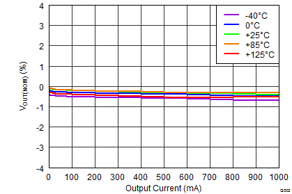
ΔVO(ΔIO) Load regulation 0 mA ≤ IO ≤ 1 A 0.3 %VO
V(DO) Dropout voltage VI = 95% VO(nom), IO = 0.5 A 216 mV
VI = 95% VO(nom), IO = 1 A 307 450 mV
I(CL) Current limit VO = 90% VO(nom) 1 1.26 A
I(GND) Ground pin current IO = 0 mA 0.58 1.0 mA
IO = 1 A 6.1 mA
I(EN) Enable pin current VEN = VI 0.78 2 µA
VI = VEN = 35 V 0.81 2 µA
I(SHDN) Shutdown supply current VEN = 0.4 V 2.55 8 µA
VEN = 0.4 V, VI = 35 V 3.04 60 µA
V+EN(HI) Enable high-level voltage 2.0 VI V
V+EN(LO) Enable low-level voltage 0.0 0.4 V
I(FB) Feedback pin current 350 nA
PSRR Power-supply rejection ratio VI = 16 V, VO(nom) = 15 V, COUT = 50 µF,
IO = 500 mA, CNR = 1 µF, f = 1 kHz
78 dB
Vn Output noise voltage VI = 3 V, VO(nom) = 1.4 V, COUT = 50 µF,
CNR = 1 µF, BW = 10 Hz to 100 kHz
4.17 µVRMS
VIN = 6 V, VO(nom) = 5 V, COUT = 50 µF,
CNR = 1 µF, BW = 10 Hz to 100 kHz
4.67 µVRMS
Tsd Thermal shutdown temperature Shutdown, temperature increasing 170 °C
Reset, temperature decreasing 150 °C
TJ Operating junction temperature –40 125 °C

6.6 Typical Characteristics

At –40°C ≤ TJ ≤ 125°C; VI = VO(nom) + 1.0 V or VI = 3.0 V (whichever is greater); VEN = VI; IO = 0 mA; CIN =10 µF; COUT = 10 µF; CNR = 1 µF; SENSE/FB tied to OUT; and 0P1V, 0P2V, 0P4V, 0P8V, 1P6V, 3P2V, 6P4V1, 6P4V2 pins OPEN, unless otherwise noted.
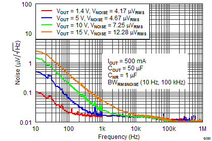
G020_BVS204.png
Figure 1. Noise vs Output Voltage
G002_BVS204.png
Figure 3. Load Regulation
G005_BVS204.png
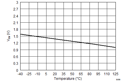
Figure 5. Enable Voltage Threshold vs Temperature
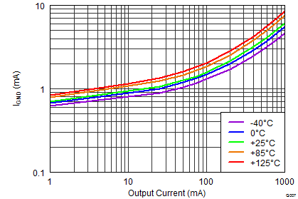
G007_BVS204.png
Figure 7. Ground Current vs Output Current
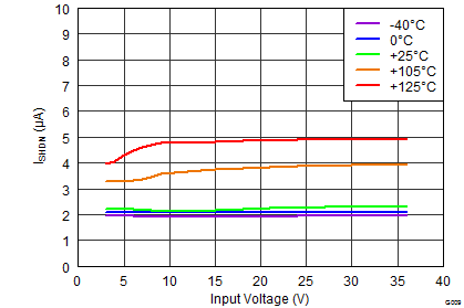
G009_BVS204.png
Figure 9. Shutdown Current vs Input Voltage
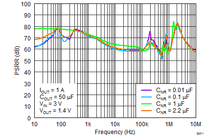
G011_BVS204.png
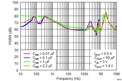
Figure 11. Power-Supply Rejection Ratio vs CNR
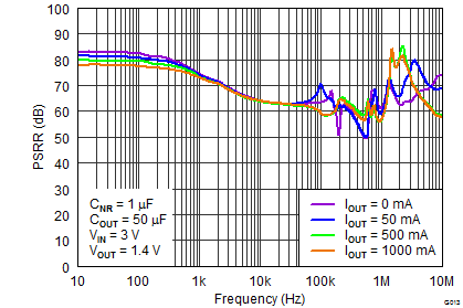
G013_BVS204.png
Figure 13. Power-Supply Rejection Ratio vs IO
G015_BVS204.png
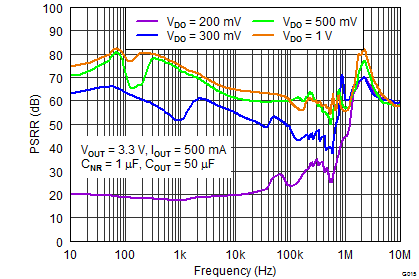
Figure 15. Power-Supply Rejection Ratio vs Dropout
G017_BVS204.png
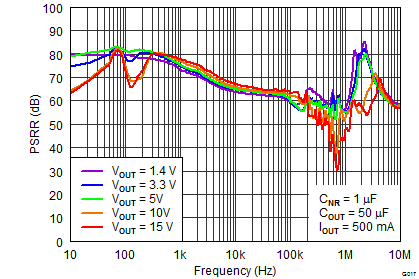
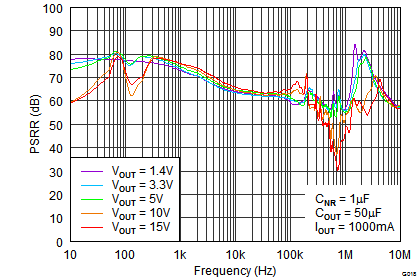
Figure 17. Power-Supply Rejection Ratio vs Output Voltage
G060_BVS204.gif
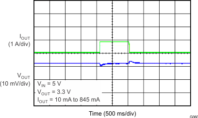
Figure 19. Load Transient
G062_BVS204.gif
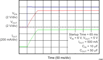
Figure 21. Startup
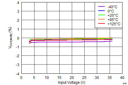
G001_BVS204.png
Figure 2. Line Regulation
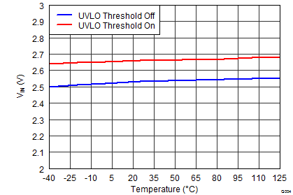
G004_BVS204.png
Figure 4. UVLO Threshold vs Temperature
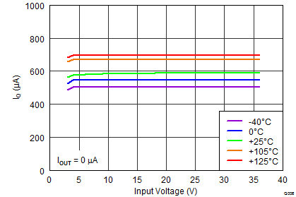
G006_BVS204.png
Figure 6. Quiescent Current vs Input Voltage
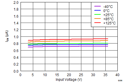
G008_BVS204.png
Figure 8. Enable Current vs Input Voltage
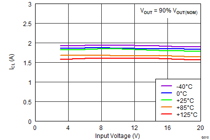
G010_BVS204.png
Figure 10. Current Limit vs Input Voltage
G012_BVS204.png
Figure 12. Power-Supply Rejection Ratio vs CNR
G014_BVS204.png
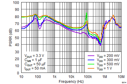
Figure 14. Power-Supply Rejection Ratio vs Dropout
G016_BVS204.png
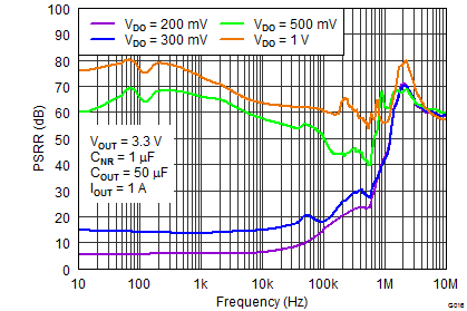
Figure 16. Power-Supply Rejection Ratio vs Dropout
G018_BVS204.png
Figure 18. Power-Supply Rejection Ratio vs Output Voltage
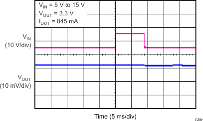
G061_BVS204.gif
Figure 20. Line Transient
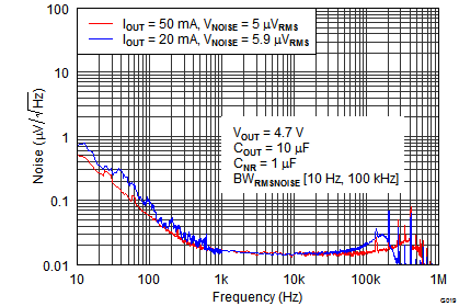
G019_BVS204.png
Figure 22. Noise vs Output Current