ZHCSG07 February 2017 TPS7A4701-EP
PRODUCTION DATA.
- 1 特性
- 2 应用
- 3 说明
- 4 修订历史记录
- 5 Pin Configuration and Functions
- 6 Specifications
- 7 Detailed Description
- 8 Application and Implementation
- 9 Power Supply Recommendations
- 10Layout
- 11器件和文档支持
- 12机械、封装和可订购信息
9 Power Supply Recommendations
The device is designed to operate from an input voltage supply range of 3 V to 35 V. If the input supply is noisy, additional input capacitors with low ESR can help improve the output noise performance.
9.1 Power Dissipation (PD)
Power dissipation must be considered in the PCB design. In order to minimize risk of device operation above 125°C, use as much copper area as available for thermal dissipation. Do not locate other power-dissipating devices near the LDO.
Power dissipation in the regulator depends on the input to output voltage difference and load conditions. PD can be calculated using Equation 7:

It is important to note that power dissipation can be minimized, and thus greater efficiency achieved, by proper selection of the system voltage rails. Proper selection allows the minimum input voltage necessary for output regulation to be obtained.
The primary heat conduction path for the QFN (RGW) package is through the thermal pad to the PCB. The thermal pad must be soldered to a copper pad area under the device. Thermal vias are recommended to improve the thermal conduction to other layers of the PCB.
The maximum power dissipation determines the maximum allowable junction temperature (TJ) for the device. Power dissipation and junction temperature are most often related by the junction-to-ambient thermal resistance (θJA) of the combined PCB and device package and the temperature of the ambient air (TA), according to Equation 8.

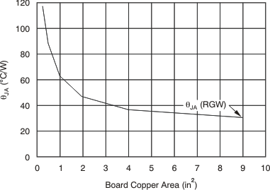
Unfortunately, this thermal resistance (θJA) depends primarily on the heat-spreading capability built into the particular PCB design, and therefore varies according to the total copper area, copper weight, and location of the spreading planes. The θJA recorded in the Thermal Information table is determined by the JEDEC standard, PCB, and copper-spreading area and is to be used only as a relative measure of package thermal performance. Note that for a well-designed thermal layout, θJA is actually the sum of the QFN package junction-to-case (bottom) thermal resistance (θJCbot) plus the thermal resistance contribution by the PCB copper. By knowing θJCbot, the minimum amount of appropriate heat sinking can be used to estimate θJA with Figure 27. θJCbot can be found in the Thermal Information table.

NOINDENT:
NOTE: θJA value at a board size of 9-in2 (that is, 3-in × 3-in) is a JEDEC standard.