SBVS121E August 2010 – May 2015 TPS7A49
PRODUCTION DATA.
- 1 Features
- 2 Applications
- 3 Description
- 4 Revision History
- 5 Pin Configuration and Functions
- 6 Specifications
- 7 Parameter Measurement Information
- 8 Detailed Description
-
9 Application and Implementation
- 9.1
Application Information
- 9.1.1 Adjustable Operation
- 9.1.2 Capacitor Recommendations
- 9.1.3 Input and Output Capacitor Requirements
- 9.1.4 Noise-Reduction and Feed-Forward Capacitor Requirements
- 9.1.5 Maximum AC Performance
- 9.1.6 Output Noise
- 9.1.7 Post DC-DC Converter Filtering
- 9.1.8 Power-Supply Rejection
- 9.1.9 Transient Response
- 9.1.10 Audio Applications
- 9.1.11 Power for Precision Analog
- 9.2 Typical Application
- 9.3 Do's and Don’ts
- 9.1
Application Information
- 10Power Supply Recommendations
- 11Layout
- 12Device and Documentation Support
- 13Mechanical, Packaging, and Orderable Information
封装选项
机械数据 (封装 | 引脚)
散热焊盘机械数据 (封装 | 引脚)
订购信息
8 Detailed Description
8.1 Overview
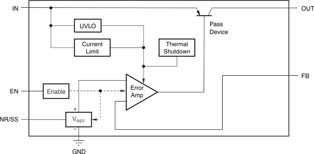
The TPS7A49 family of devices are wide VIN, low-noise, 150-mA linear regulators (LDOs). These devices feature an enable pin, programmable soft-start, current limiting, and thermal protection circuitry that allow the device to be used in a wide variety of applications. As bipolar-based devices, the TPS7A49 family are ideal for high-accuracy, high-precision applications at higher voltages.
8.3 Feature Description
8.3.1 Internal Current Limit
The fixed internal current limit of the TPS7A49 family helps protect the regulator during fault conditions. The maximum amount of current the device can source is the current limit (309 mA, typical), and is largely independent of output voltage. For reliable operation, the device does not operate in current limit for extended periods of time.
8.3.2 Programmable Soft-Start
The NR capacitor also functions as a soft-start capacitor to slow down the rise time of the output. The rise time of the output when using an NR capacitor is governed by Equation 1. In Equation 1, tSS is the soft-start time in milliseconds, and CNR/SS is the capacitance at the NR pin in nanofarads.

8.3.3 Enable Pin Operation
The TPS7A49 provides an enable feature (EN) that turns on the regulator when VEN > VEN(high) and disables the device when VEN < VEN(low).
8.3.4 Thermal Protection
Thermal protection disables the output when the junction temperature rises to approximately 170°C, allowing the device to cool. When the junction temperature cools to approximately 150°C, the output circuitry is enabled. Depending on power dissipation, thermal resistance, and ambient temperature, the thermal protection circuit can cycle on and off. This cycling limits the dissipation of the regulator, protecting it from damage as a result of overheating.
Any tendency to activate the thermal protection circuit indicates excessive power dissipation or an inadequate heatsink. For reliable operation, limit junction temperature to a maximum of 125°C. To estimate the margin of safety in a complete design (including heatsink), increase the ambient temperature until the thermal protection is triggered; use worst-case loads and signal conditions. For good reliability, trigger thermal protection at least 45°C above the maximum expected ambient condition of a particular application. This configuration produces a worst-case junction temperature of 125°C at the highest expected ambient temperature and worst-case load.
The internal protection circuitry of the TPS7A49 is designed to protect against overload conditions. The protection circuitry is not intended to replace proper heatsinking. Continuously running the TPS7A49 into thermal shutdown degrades device reliability.
8.4 Device Functional Modes
8.4.1 Normal Operation
The device regulates to the nominal output voltage under the following conditions:
- The input voltage is at least as high as VIN(min).
- The input voltage is greater than the nominal output voltage added to the dropout voltage.
- The enable voltage has previously exceeded the enable rising threshold voltage and has not decreased below the enable falling threshold.
- The output current is less than the current limit.
- The device junction temperature is less than the maximum specified junction temperature.
8.4.2 Dropout Operation
If the input voltage is lower than the nominal output voltage plus the specified dropout voltage, but all other conditions are met for normal operation, the device operates in dropout mode. In this mode of operation, the output voltage is the same as the input voltage minus the dropout voltage. The transient performance of the device is significantly degraded because the pass device (such as a bipolar junction transistor, or BJT) is in saturation and no longer controls the current through the LDO. Line or load transients in dropout can result in large output voltage deviations.
8.4.3 Disabled
The device is disabled under the following conditions:
- The enable voltage is less than the enable falling threshold voltage or has not yet exceeded the enable rising threshold.
- The device junction temperature is greater than the thermal shutdown temperature.
Table 1 lists the conditions that lead to the different modes of operation.
