ZHCSHE2B September   2017  – June 2018 TPS7A52-Q1

PRODUCTION DATA.  

  1. 特性
  2. 应用
  3. 说明
    1.     Device Images
      1.      为射频组件供电
      2.      输出电压噪声与频率和输出电压间的关系
  4. 修订历史记录
  5. Pin Configuration and Functions
    1.     Pin Functions
  6. Specifications
    1. 6.1 Absolute Maximum Ratings
    2. 6.2 ESD Ratings
    3. 6.3 Recommended Operating Conditions
    4. 6.4 Thermal Information
    5. 6.5 Electrical Characteristics
    6. 6.6 Typical Characteristics
  7. Detailed Description
    1. 7.1 Overview
    2. 7.2 Functional Block Diagram
    3. 7.3 Feature Description
      1. 7.3.1 Voltage Regulation Features
        1. 7.3.1.1 DC Regulation
        2. 7.3.1.2 AC and Transient Response
      2. 7.3.2 System Start-Up Features
        1. 7.3.2.1 Programmable Soft Start (NR/SS Pin)
        2. 7.3.2.2 Internal Sequencing
          1. 7.3.2.2.1 Enable (EN)
          2. 7.3.2.2.2 Undervoltage Lockout (UVLO) Control
          3. 7.3.2.2.3 Active Discharge
        3. 7.3.2.3 Power-Good Output (PG)
      3. 7.3.3 Internal Protection Features
        1. 7.3.3.1 Foldback Current Limit (ICL)
        2. 7.3.3.2 Thermal Protection (Tsd)
    4. 7.4 Device Functional Modes
      1. 7.4.1 Regulation
      2. 7.4.2 Disabled
      3. 7.4.3 Current Limit Operation
  8. Application and Implementation
    1. 8.1 Application Information
      1. 8.1.1  Recommended Capacitor Types
        1. 8.1.1.1 Input and Output Capacitor Requirements (CIN and COUT)
        2. 8.1.1.2 Noise-Reduction and Soft-Start Capacitor (CNR/SS)
        3. 8.1.1.3 Feed-Forward Capacitor (CFF)
      2. 8.1.2  Soft-Start and Inrush Current
      3. 8.1.3  Optimizing Noise and PSRR
      4. 8.1.4  Charge Pump Noise
      5. 8.1.5  Current Sharing
      6. 8.1.6  Adjustable Operation
      7. 8.1.7  Power-Good Operation
      8. 8.1.8  Undervoltage Lockout (UVLO) Operation
      9. 8.1.9  Dropout Voltage (VDO)
      10. 8.1.10 Load Transient Response
      11. 8.1.11 Reverse Current Protection Considerations
      12. 8.1.12 Power Dissipation (PD)
      13. 8.1.13 Estimating Junction Temperature
    2. 8.2 Typical Application
      1. 8.2.1 Design Requirements
      2. 8.2.2 Detailed Design Procedure
      3. 8.2.3 Application Curves
  9. Power Supply Recommendations
  10. 10Layout
    1. 10.1 Layout Guidelines
      1. 10.1.1 Board Layout
      2. 10.1.2 RTK Package—High CTE Mold Compound
    2. 10.2 Layout Example
  11. 11器件和文档支持
    1. 11.1 器件支持
      1. 11.1.1 开发支持
        1. 11.1.1.1 评估模块
        2. 11.1.1.2 参考设计
        3. 11.1.1.3 Spice 模型
      2. 11.1.2 器件命名规则
    2. 11.2 文档支持
      1. 11.2.1 相关文档
    3. 11.3 接收文档更新通知
    4. 11.4 社区资源
    5. 11.5 商标
    6. 11.6 静电放电警告
    7. 11.7 术语表
  12. 12机械、封装和可订购信息

封装选项

机械数据 (封装 | 引脚)
散热焊盘机械数据 (封装 | 引脚)
订购信息

Typical Characteristics

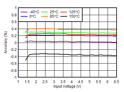
at TA = 25°C, VIN = 1.4 V or VIN = VOUT(NOM) + 0.4 V (whichever is greater), VBIAS = open, VOUT(NOM) = 0.8 V, VEN = 1.1 V, COUT = 22 µF, CNR/SS = 0 nF, CFF = 0 nF, and PG pin pulled up to VIN with 100 kΩ (unless otherwise noted)
TPS7A52-Q1 Fig1-PSRRvsFrequencyandIout.gif
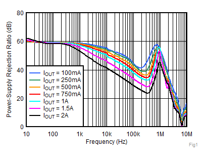
VIN = 1.1 V, VBIAS = 5 V, CNR/SS = 10 nF, CFF = 10 nF
Figure 1. PSRR vs Frequency and IOUT
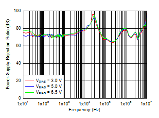
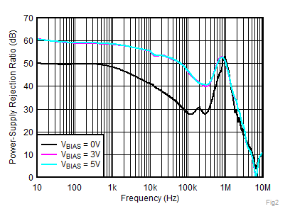
TPS7A52-Q1 Fig3-PSRRvsFrequencyandVbias.gif
VIN = 1.4 V, IOUT = 1 A,
CNR/SS = 10 nF, CFF = 10 nF
Figure 3. PSRR vs Frequency and VBIAS
TPS7A52-Q1 Fig5-PSRRvsFrequencyandVout=Vin_plus0.3V.gif
VIN = VOUT + 0.3 V, VBIAS = 5.0 V, IOUT = 2 A,
CNR/SS = 10 nF, CFF = 10 nF
Figure 5. PSRR vs Frequency and VOUT With Bias
TPS7A52-Q1 Fig7-PSRRvsFrequencyandCout.gif
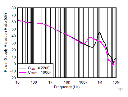
VIN = VOUT + 0.3 V, VOUT = 1 V, IOUT = 2 A,
CNR/SS = 10 nF, CFF = 10 nF
Figure 7. PSRR vs Frequency and COUT
TPS7A52-Q1 Fig9-OutputVoltageNoisevsOutputVoltage.gif
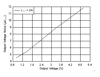
VIN = VOUT + 0.3 V and VBIAS = 5 V for VOUT ≤ 2.2 V,
CNR/SS = 10 nF, CFF = 10 nF,
RMS noise BW = 10 Hz to 100 kHz
Figure 9. Output Voltage Noise vs Output Voltage
TPS7A52-Q1 Fig11-OutputVoltageNoisevsFreqvsVin.gif
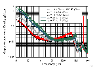
IOUT = 2 A, CNR/SS = 10 nF, CFF = 10 nF,
RMS noise BW = 10 Hz to 100 kHz
Figure 11. Output Noise vs Frequency and VIN
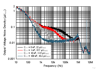
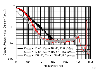
TPS7A52-Q1 Fig13-OutputVoltageNoisevsFreqvsCff.gif
VIN = VOUT + 0.3 V, VBIAS = 5 V, IOUT = 2 A, sequencing with a dc-dc converter and PG,
CNR/SS = 10 nF, RMS noise BW = 10 Hz to 100 kHz
Figure 13. Output Noise vs Frequency and CFF
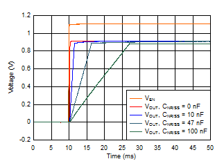
TPS7A52-Q1 Startup_Vs_Cnr.gif
VIN = 1.2 V, VOUT = 0.9 V, VBIAS = 5.0 V, IOUT = 2 A,
CFF = 10 nF
Figure 15. Start-Up Waveform vs Time and CNR/SS
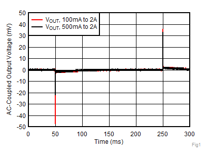
TPS7A52-Q1 Load_trans_vs_Vout_no_bias.gif
IOUT, DC = 100 mA,
CNR/SS = CFF = 10 nF, slew rate = 1 A/µs
Figure 17. Load Transient vs Time and VOUT Without Bias
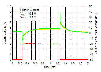
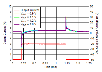
TPS7A52-Q1 Fig19-LoadtransientVout=5VvsDCload.gif
RGR package, VOUT = 0.9 V, VIN = 1.2 V, VBIAS = 5.0 V,
CNR/SS = CFF = 10 nF, slew rate = 1 A/µs
Figure 19. Load Transient vs Time and DC Load
TPS7A52-Q1 D021-SBVS296-01.gif
RGR package, IOUT = 2 A, VBIAS = 6.5 V
Figure 21. Dropout Voltage vs Input Voltage With Bias
TPS7A52-Q1 D023-SBVS296-01.gif
RGR package, VIN = 1.1 V, VBIAS = 3 V
Figure 23. Dropout Voltage vs Output Current With Bias
TPS7A52-Q1 D026-SBVS296-01.gif
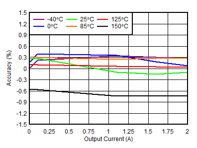
VIN = 1.4 V, VBIAS = 0 V
Figure 25. Load Regulation With Bias
TPS7A52-Q1 D032-SBVS296-02.gif
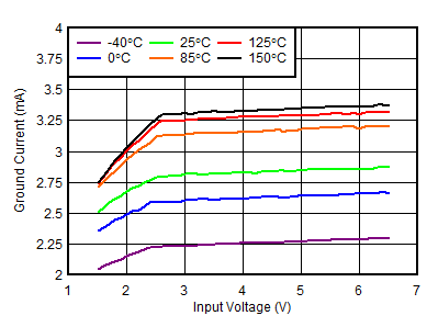
VBIAS = 0 V, IOUT = 5 mA
Figure 27. Ground Current vs Input Voltage
TPS7A52-Q1 D034-SBVS296-02.gif
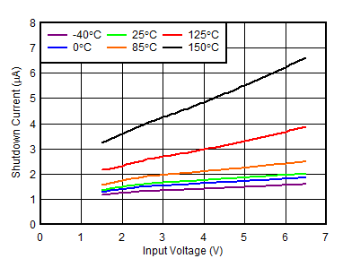
VBIAS = 0 V
Figure 29. Shutdown Current vs Input Voltage
TPS7A52-Q1 D036-SBVS296-01.gif
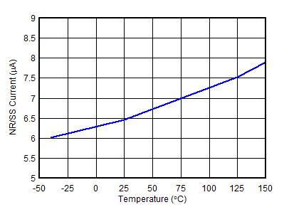
VBIAS = 0 V
Figure 31. NR/SS Current vs Temperature
TPS7A52-Q1 D038-SBVS296-02.gif
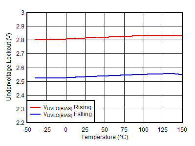
VIN = 1.1 V
Figure 33. VBIAS UVLO vs Temperature
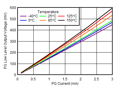
TPS7A52-Q1 D040-SBVS296-02.gif
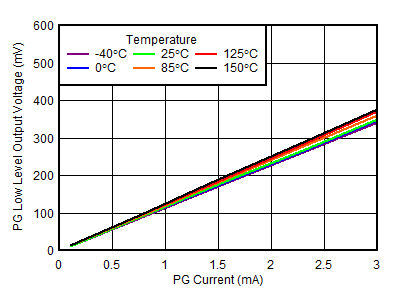
Figure 35. PG Voltage vs PG Current Sink
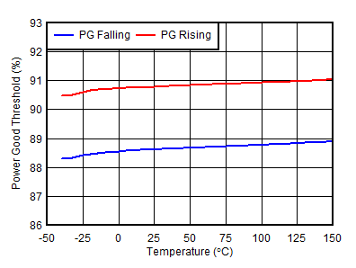
TPS7A52-Q1 D042-SBVS296-01.gif
Figure 37. PG Threshold vs Temperature
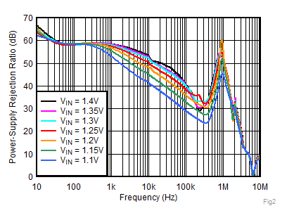
TPS7A52-Q1 Fig2-PSRRvsFrequencyandVin.gif
IOUT = 2 A, VBIAS = 5 V,
CNR/SS = 10 nF, CFF = 10 nF
Figure 2. PSRR vs Frequency and VIN With Bias
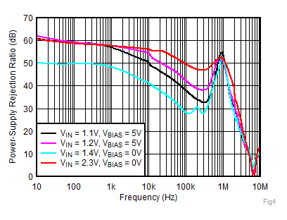
TPS7A52-Q1 Fig4-PSRRvsFrequencyandVin_Vbias.gif
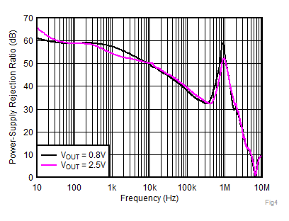
IOUT = 1 A,
CNR/SS = 10 nF, CFF = 10 nF
Figure 4. PSRR vs Frequency and VIN
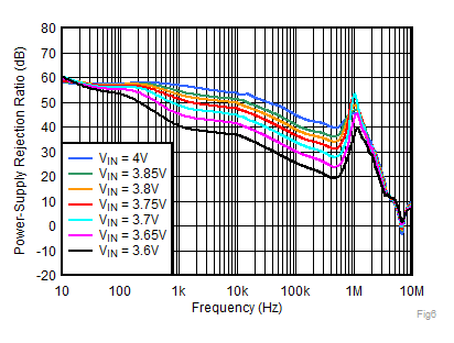
TPS7A52-Q1 Fig6-PSRRvsFrequencyandVin,Vout=3.3V.gif
VOUT = 3.3 V, IOUT = 2 A,
CNR/SS = 10 nF, CFF = 10 nF
Figure 6. PSRR vs Frequency and VIN for VOUT = 3.3 V
TPS7A52-Q1 7a84_Bias_PSRR.gif
VIN = VOUT + 0.3 V, VOUT = 1 V, IOUT = 2 A,
CNR/SS = 10 nF, CFF = 10 nF
Figure 8. VBIAS PSRR vs Frequency and VBIAS
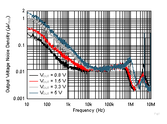
TPS7A52-Q1 Fig10-OutputVoltageNoisevsFreqvsVout.gif
VIN = VOUT + 0.3 V and VBIAS = 5 V for VOUT ≤ 2.2 V, IOUT = 2 A,, CNR/SS = 10 nF, CFF = 10 nF,
RMS noise BW = 10 Hz to 100 kHz
Figure 10. Output Noise vs Frequency and VOUT
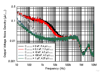
TPS7A52-Q1 Fig12-OutputVoltageNoisevsFreqvsCnrss.gif
VIN = VOUT + 0.3 V, VBIAS = 5 V, IOUT = 2 A,
CFF = 10 nF, RMS noise BW = 10 Hz to 100 kHz
Figure 12. Output Noise vs Frequency and CNR/SS
TPS7A52-Q1 Fig14-OutputVoltageNoisevsFreqvsCnrss-CffVout=5V.gif
VOUT = 5 V, IOUT = 2 A, CFF = 10 nF,
RMS noise BW = 10 Hz to 100 kHz
Figure 14. Output Noise at VOUT = 5 V
TPS7A52-Q1 Load_trans_vs_Vout.gif
VIN = VOUT + 0.3 V, VBIAS = 5 V, IOUT, DC = 100 mA, slew rate = 1 A/µs, CNR/SS = CFF = 10 nF
Figure 16. Load Transient vs Time and VOUT With Bias
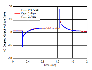
TPS7A52-Q1 Load_trans_vs_SR.gif
VOUT = 5 V, IOUT, DC = 100 mA, IOUT = 100 mA to 2 A,
CNR/SS = CFF = 10 nF
Figure 18. Load Transient vs Time and Slew Rate
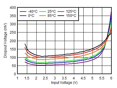
TPS7A52-Q1 D020-SBVS296-01.gif
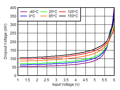
IOUT = 2 A, VBIAS = 0 V
Figure 20. Dropout Voltage vs Input Voltage Without Bias
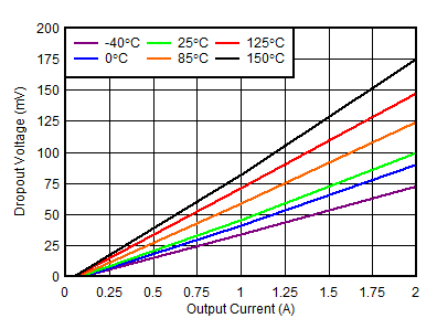
TPS7A52-Q1 D022-SBVS296-01.gif
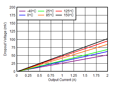
RGR package, VIN = 1.4 V, VBIAS = 0 V
Figure 22. Dropout Voltage vs Output Current Without Bias
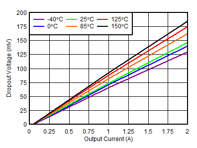
TPS7A52-Q1 D024-SBVS296-01.gif
RGR package, VIN = 5.5 V
Figure 24. Dropout Voltage vs Output Current (High VIN)
TPS7A52-Q1 D029-SBVS296-01.gif
VOUT = 0.8 V, VBIAS = 0 V, IOUT = 5 mA
Figure 26. Line Regulation Without Bias
TPS7A52-Q1 D033-SBVS296-01.gif
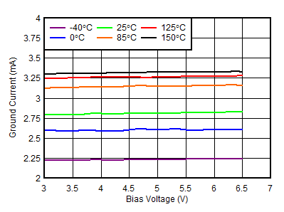
VIN = 1.1 V, IOUT = 5 mA
Figure 28. Ground Current vs Bias Voltage
TPS7A52-Q1 D035-SBVS296-01.gif
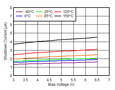
VIN = 1.1 V
Figure 30. Shutdown Current vs Bias Voltage
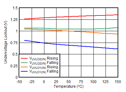
TPS7A52-Q1 D037-SBVS296-02.gif
Figure 32. VIN UVLO vs Temperature
TPS7A52-Q1 D039-SBVS296-01.gif
VIN = 1.4 V, 6.5 V
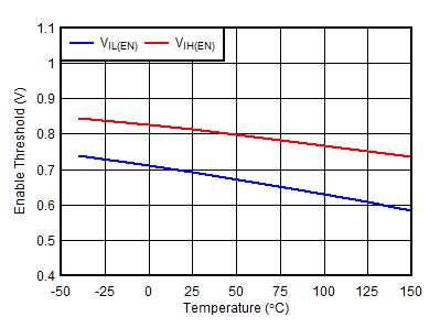
Figure 34. Enable Threshold vs Temperature
TPS7A52-Q1 D041-SBVS296-01.gif
VIN = 6.5 V
Figure 36. PG Voltage vs PG Current Sink
TPS7A52-Q1 D043-SBVS296-01.gif
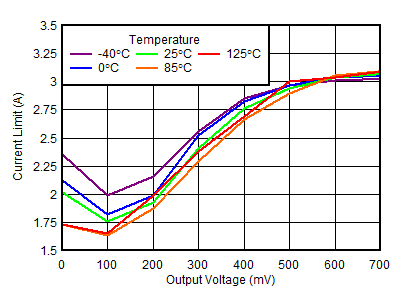
Temperature limited because of power dissipation
Figure 38. Foldback Current Limit vs Output Voltage