ZHCSKH2 November 2019 TPS7A52
ADVANCE INFORMATION for pre-production products; subject to change without notice.
- 1 特性
- 2 应用
- 3 说明
- 4 修订历史记录
- 5 Pin Configuration and Functions
- 6 Specifications
- 7 Detailed Description
-
8 Application and Implementation
- 8.1
Application Information
- 8.1.1 Recommended Capacitor Types
- 8.1.2 Soft Start and Inrush Current
- 8.1.3 Optimizing Noise and PSRR
- 8.1.4 Charge Pump Noise
- 8.1.5 Current Sharing
- 8.1.6 Adjustable Operation
- 8.1.7 Power-Good Operation
- 8.1.8 Undervoltage Lockout (UVLO) Operation
- 8.1.9 Dropout Voltage (VDO)
- 8.1.10 Device Behavior During Transition From Dropout Into Regulation
- 8.1.11 Load Transient Response
- 8.1.12 Reverse Current Protection Considerations
- 8.1.13 Power Dissipation (PD)
- 8.1.14 Estimating Junction Temperature
- 8.2 Typical Application
- 8.1
Application Information
- 9 Power Supply Recommendations
- 10Layout
- 11器件和文档支持
- 12机械、封装和可订购信息
8.1.8 Undervoltage Lockout (UVLO) Operation
The UVLO circuit makes sure that the device remains disabled before the input or bias supplies reach the minimum operational voltage range, and that the device shuts down when the input supply or bias supply falls too low.
The UVLO circuit has a minimum response time of several microseconds to fully assert. During this time, a downward line transient below approximately 0.8 V causes the UVLO to assert for a short time; however, the UVLO circuit does not have enough stored energy to fully discharge the internal circuits inside of the device. When the UVLO circuit does not fully discharge, the internal circuits of the output are not fully disabled.
The effect of the downward line transient can be mitigated by either using a larger input capacitor to limit the fall time of the input supply when operating near the minimum VIN, or by using a bias rail.
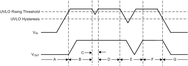
Figure 6 shows the UVLO circuit response to various input voltage events. The diagram can be separated into the following regions:
- Region A: The device does not turn on until the input reaches the UVLO rising threshold.
- Region B: Normal operation with a regulated output.
- Region C: Brownout event above the UVLO falling threshold (UVLO rising threshold – UVLO hysteresis). The output may fall out of regulation but the device is still enabled.
- Region D: Normal operation with a regulated output.
- Region E: Brownout event below the UVLO falling threshold. The device is disabled in most cases and the output falls because of the load and active discharge circuit. The device is reenabled when the UVLO rising threshold is reached by the input voltage and a normal start-up then follows.
- Region F: Normal operation followed by the input falling to the UVLO falling threshold.
- Region G: The device is disabled when the input voltage falls below the UVLO falling threshold to 0 V. The output falls because of the load and active discharge circuit.
 Figure 6. Typical UVLO Operation