ZHCSKH2 November 2019 TPS7A52
ADVANCE INFORMATION for pre-production products; subject to change without notice.
- 1 特性
- 2 应用
- 3 说明
- 4 修订历史记录
- 5 Pin Configuration and Functions
- 6 Specifications
- 7 Detailed Description
-
8 Application and Implementation
- 8.1
Application Information
- 8.1.1 Recommended Capacitor Types
- 8.1.2 Soft Start and Inrush Current
- 8.1.3 Optimizing Noise and PSRR
- 8.1.4 Charge Pump Noise
- 8.1.5 Current Sharing
- 8.1.6 Adjustable Operation
- 8.1.7 Power-Good Operation
- 8.1.8 Undervoltage Lockout (UVLO) Operation
- 8.1.9 Dropout Voltage (VDO)
- 8.1.10 Device Behavior During Transition From Dropout Into Regulation
- 8.1.11 Load Transient Response
- 8.1.12 Reverse Current Protection Considerations
- 8.1.13 Power Dissipation (PD)
- 8.1.14 Estimating Junction Temperature
- 8.2 Typical Application
- 8.1
Application Information
- 9 Power Supply Recommendations
- 10Layout
- 11器件和文档支持
- 12机械、封装和可订购信息
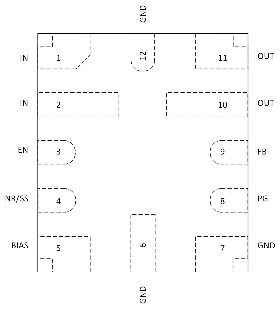
5 Pin Configuration and Functions
RPS Package
2.2-mm × 2.5-mm, 12-Pin VQFN
Top View

Pin Functions
| PIN | DESCRIPTION | ||
|---|---|---|---|
| NAME | NO. | I/O | |
| BIAS | 5 | I | BIAS supply voltage. This pin enables the use of low-input voltage, low-output (LILO) voltage conditions (that is, VIN = 1.2 V, VOUT = 1 V) to reduce power dissipation across the die. The use of a BIAS voltage improves dc and ac performance for VIN ≤ 2.2 V. A 10-µF capacitor or larger must be connected between this pin and ground. If not used, this pin must be left floating or tied to ground. |
| EN | 3 | I | Enable pin. Driving this pin to logic high enables the device; driving this pin to logic low disables the device. If enable functionality is not required, this pin must be connected to IN or BIAS. |
| FB | 9 | I | Feedback pin connected to the error amplifier. Although not required, a 10-nF feed-forward capacitor from FB to OUT (as close to the device as possible) is recommended to maximize ac performance. The use of a feed-forward capacitor can disrupt PG (power good) functionality. |
| GND | 6, 7, 12 | — | Ground pin. These pins must be connected to ground, the thermal pad, and each other with a low-impedance connection. |
| IN | 1, 2 | I | Input supply voltage pin. A 10-µF or larger ceramic capacitor (5 µF or greater of capacitance) from IN to ground is recommended to reduce the impedance of the input supply. Place the input capacitor as close to the input as possible. |
| NR/SS | 4 | — | Noise-reduction and soft-start pin. Connecting an external capacitor between this pin and ground reduces reference voltage noise and also enables the soft-start function. Although not required, a 10-nF or larger capacitor is recommended to be connected from NR/SS to GND (as close to the pin as possible) to maximize ac performance. |
| OUT | 10, 11 | O | Regulated output pin. A 47-µF or larger ceramic capacitor (25 µF or greater of capacitance) from OUT to ground is required for stability and must be placed as close to the output as possible. Minimize the impedance from the OUT pin to the load. |
| PG | 8 | O | Active-high, power-good pin. An open-drain output indicates when the output voltage reaches VIT(PG) of the target. The use of a feed-forward capacitor can disrupt PG (power good) functionality. |