ZHCSQT5 July 2022 TPS7A57
PRODUCTION DATA
- 1 特性
- 2 应用
- 3 说明
- 4 Revision History
- 5 Pin Configuration and Functions
- 6 Specifications
-
7 Detailed Description
- 7.1 Overview
- 7.2 Functional Block Diagram
- 7.3
Feature Description
- 7.3.1 Output Voltage Setting and Regulation
- 7.3.2 Low-Noise, Ultra-High Power-Supply Rejection Ratio (PSRR)
- 7.3.3 Programmable Soft-Start (NR/SS Pin)
- 7.3.4 Precision Enable and UVLO
- 7.3.5 Charge Pump Enable and BIAS Rail
- 7.3.6 Power-Good Pin (PG Pin)
- 7.3.7 Active Discharge
- 7.3.8 Thermal Shutdown Protection (TSD)
- 7.4 Device Functional Modes
-
8 Application and Implementation
- 8.1
Application Information
- 8.1.1 Precision Enable (External UVLO)
- 8.1.2 Undervoltage Lockout (UVLO) Operation
- 8.1.3 Dropout Voltage (VDO)
- 8.1.4 Input and Output Capacitor Requirements (CIN and COUT)
- 8.1.5 Recommended Capacitor Types
- 8.1.6 Soft-Start, Noise Reduction (NR/SS Pin), and Power-Good (PG Pin)
- 8.1.7 Optimizing Noise and PSRR
- 8.1.8 Adjustable Operation
- 8.1.9 Load Transient Response
- 8.1.10 Current Limit and Foldback Behavior
- 8.1.11 Charge Pump Operation
- 8.1.12 Sequencing
- 8.1.13 Power-Good Functionality
- 8.1.14 Output Impedance
- 8.1.15 Paralleling for Higher Output Current and Lower Noise
- 8.1.16 Current Mode Margining
- 8.1.17 Voltage Mode Margining
- 8.1.18 Power Dissipation (PD)
- 8.1.19 Estimating Junction Temperature
- 8.1.20 TPS7A57EVM-081 Thermal Analysis
- 8.2 Typical Application
- 8.3 Power Supply Recommendations
- 8.4 Layout
- 8.1
Application Information
- 9 Device and Documentation Support
- 10Mechanical, Packaging, and Orderable Information
8.1.6 Soft-Start, Noise Reduction (NR/SS Pin), and Power-Good (PG Pin)
The NR/SS pin has the dual function of controlling the soft-start time and reducing the noise generated by the internal band-gap reference and the external resistor RREF. The NR/SS capacitor (CNR/SS) reduces the output noise to very low levels and sets the output ramp rate to limit inrush current.
The device features a programmable, monotonic, voltage-controlled, soft-start circuit that is set to work with an external capacitor (CNR/SS). In addition to the soft-start feature, the CNR/SS capacitor also lowers the output voltage noise of the LDO. The soft-start feature can be used to eliminate power-up initialization problems. The controlled output voltage ramp also reduces peak inrush current during start up, minimizing start-up transients to the input power bus.
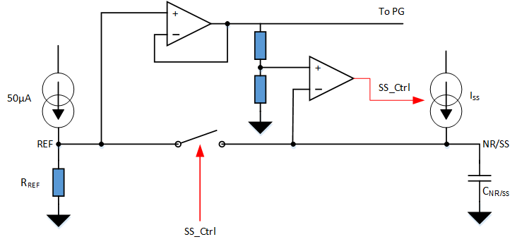
To achieve a monotonic start up, the device output voltage tracks the VNR/SS reference voltage until this reference reaches its set value (the set output voltage). The VNR/SS reference voltage is set by the RREF resistor and, during start up, the device uses a fast charging current (IFAST_SS), as shown in Figure 8-4, to charge the CNR/SS capacitor.
 Figure 8-4 Simplified Soft-Start
Circuit
Figure 8-4 Simplified Soft-Start
CircuitThe 200-μA (typical) INR/SS current quickly charges CNR/SS until its voltage reaches approximately 97% of the set output voltage, then the ISS current turns off, the switch between REF and NR/SS closes, and only the IREF current continues to charge CNR/SS to its set output voltage level.
The soft-start ramp time depends on the fast start-up (INR/SS) charging current, the reference current (IREF), CNR/SS capacitor value, and the targeted output voltage (VOUT(target)). Equation 3 calculates the soft-start ramp time.
The ISS current is provided in the Section 6.6 section and has a value of 200 μA (typical). The IREF current has a value of 50 μA (typical). The remaining 3% of the start-up time is determined by the RREF × CNR/SS time constant. Figure 8-5 shows the PG threshold at start up.
 Figure 8-5 PG Threshold During
Start-Up
Figure 8-5 PG Threshold During
Start-UpThe output voltage noise can be lowered significantly by increasing the CNR/SS capacitor. The CNR/SS capacitor and RREF resistor form a low-pass filter (LPF) that filters out noise from the VREF voltage reference, thereby reducing the device noise floor. The LPF is a single-pole filter and Equation 4 calculates the LPF cutoff frequency. Increasing the CNR/SS capacitor can significantly lower output voltage noise, however, doing so lengthens start-up time. For low-noise applications, use a 4.7-μF CNR/SS for optimal noise and start-up time trade off.
Figure 8-6 and Figure 8-7 show the impact of the CNR/SS capacitor on the LDO output voltage noise.

| CIN = 4.7 μF, COUT = 22 μF,
VCP_EN = VIN, VIN =
5.3 V, VOUT = 5 V, IOUT = 5 A |

| CIN = 4.7 μF, COUT = 22 μF,
VIN = 5.3 V, VOUT = 5 V, VBIAS = 11 V |