ZHCSQT5 July 2022 TPS7A57
PRODUCTION DATA
- 1 特性
- 2 应用
- 3 说明
- 4 Revision History
- 5 Pin Configuration and Functions
- 6 Specifications
-
7 Detailed Description
- 7.1 Overview
- 7.2 Functional Block Diagram
- 7.3
Feature Description
- 7.3.1 Output Voltage Setting and Regulation
- 7.3.2 Low-Noise, Ultra-High Power-Supply Rejection Ratio (PSRR)
- 7.3.3 Programmable Soft-Start (NR/SS Pin)
- 7.3.4 Precision Enable and UVLO
- 7.3.5 Charge Pump Enable and BIAS Rail
- 7.3.6 Power-Good Pin (PG Pin)
- 7.3.7 Active Discharge
- 7.3.8 Thermal Shutdown Protection (TSD)
- 7.4 Device Functional Modes
-
8 Application and Implementation
- 8.1
Application Information
- 8.1.1 Precision Enable (External UVLO)
- 8.1.2 Undervoltage Lockout (UVLO) Operation
- 8.1.3 Dropout Voltage (VDO)
- 8.1.4 Input and Output Capacitor Requirements (CIN and COUT)
- 8.1.5 Recommended Capacitor Types
- 8.1.6 Soft-Start, Noise Reduction (NR/SS Pin), and Power-Good (PG Pin)
- 8.1.7 Optimizing Noise and PSRR
- 8.1.8 Adjustable Operation
- 8.1.9 Load Transient Response
- 8.1.10 Current Limit and Foldback Behavior
- 8.1.11 Charge Pump Operation
- 8.1.12 Sequencing
- 8.1.13 Power-Good Functionality
- 8.1.14 Output Impedance
- 8.1.15 Paralleling for Higher Output Current and Lower Noise
- 8.1.16 Current Mode Margining
- 8.1.17 Voltage Mode Margining
- 8.1.18 Power Dissipation (PD)
- 8.1.19 Estimating Junction Temperature
- 8.1.20 TPS7A57EVM-081 Thermal Analysis
- 8.2 Typical Application
- 8.3 Power Supply Recommendations
- 8.4 Layout
- 8.1
Application Information
- 9 Device and Documentation Support
- 10Mechanical, Packaging, and Orderable Information
8.1.16 Current Mode Margining
Output voltage margining is a technique that allows a circuit to be evaluated for how well changes are tolerated in the power supply. This test is typically performed by adjusting the supply voltage to a fixed percentage above and below its nominal output voltage.
This section discusses the implementation of a voltage margining application using the TPS7A57. A margining target of ±2.5% is used to demonstrate the chosen implementation.
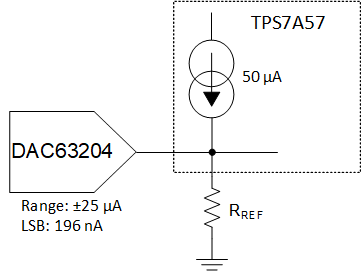
Figure 8-23 shows a simplified visualization of the TPS7A57 REF pin with a current DAC.
 Figure 8-23 Simplified Margining
Schematic
Figure 8-23 Simplified Margining
SchematicTable 8-7 summarizes the design requirements.
| PARAMETER | Design Values |
|---|---|
| VIN | 2.5 V |
| VOUT | 1.8 V nominal with ±2.5% margining |
| CNR/SS | 4.7 μF |
| RREF | 36 kΩ |
| DAC IOUT range | ±25 μA |
In this example, the output voltage is set to a nominal 1.8 V using 36 kΩ at the REF pin to GND. Equation 12 calculates the RREF resistor value.
The DAC63204, a 4-channel, 12-bit voltage and current output DAC with I2C, was selected and programmed into the current-output mode with an output range set to ±25 μA. In conjunction with the 8-bit current DAC resolution, this output range allows a minimum step size (or LSB) of approximately 196 nA. Into the 36-kΩ resistor, the LSB translates into a 7-mV voltage resolution or 0.38% of the nominal 1.8-V targeted voltage. To achieve the full ±2.5% swing around the nominal voltage, the DAC63204 must source or sink ±1.25 μA.
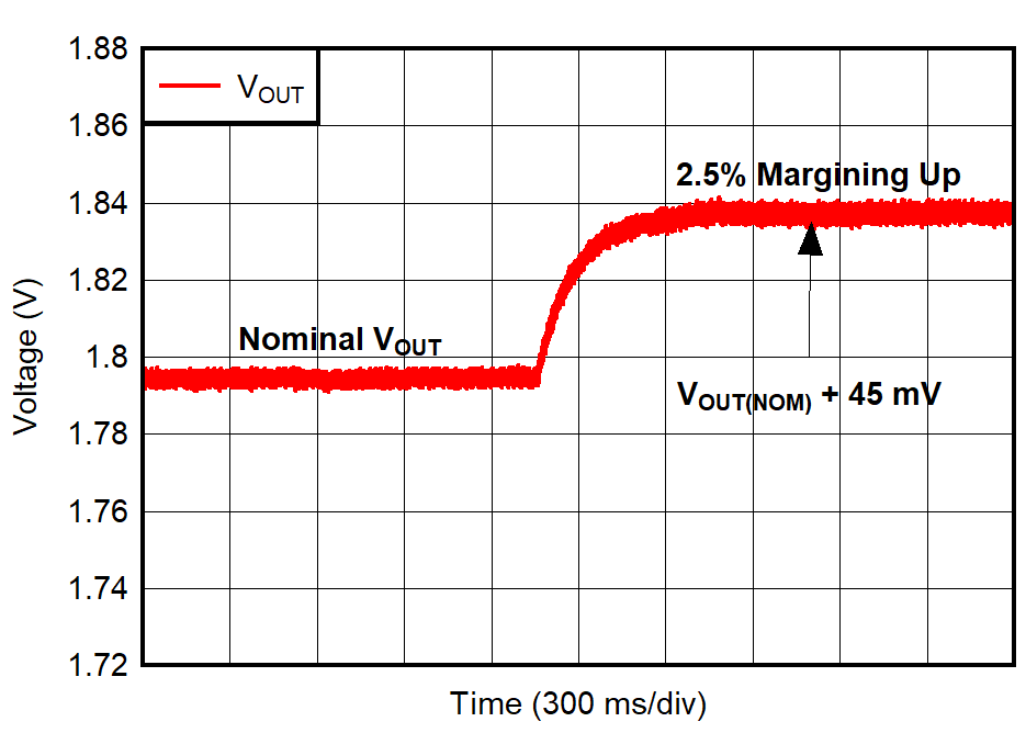
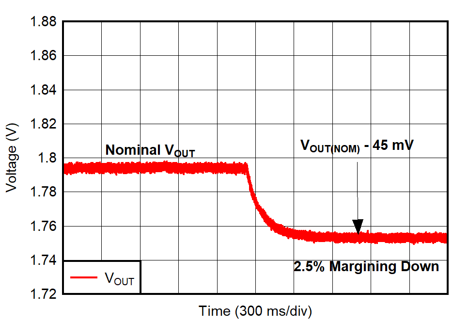
The current flowing through RREF changes to 51.25 μA and 48.75 μA and adjusts the output voltage to 1.845 V and 1.75 V, respectively.
Figure 8-24 and Figure 8-25 show the current margining results.
 Figure 8-24 Margining Up
 Figure 8-25 Margining Down
When implementing voltage margining with this LDO, a time constant is associated with its response. This RC time constant is a result of the parallel combination of RREF and CNR/SS, see Figure 8-23. This RC effect is illustrated in Figure 8-24 and Figure 8-25.
Equation 13 calculates the time constant for this implementation:
where:
- RREF is 36 kΩ
- CNR/SS is 4.7 μF
- τ = 169 ms