ZHCSQT5 July 2022 TPS7A57
PRODUCTION DATA
- 1 特性
- 2 应用
- 3 说明
- 4 Revision History
- 5 Pin Configuration and Functions
- 6 Specifications
-
7 Detailed Description
- 7.1 Overview
- 7.2 Functional Block Diagram
- 7.3
Feature Description
- 7.3.1 Output Voltage Setting and Regulation
- 7.3.2 Low-Noise, Ultra-High Power-Supply Rejection Ratio (PSRR)
- 7.3.3 Programmable Soft-Start (NR/SS Pin)
- 7.3.4 Precision Enable and UVLO
- 7.3.5 Charge Pump Enable and BIAS Rail
- 7.3.6 Power-Good Pin (PG Pin)
- 7.3.7 Active Discharge
- 7.3.8 Thermal Shutdown Protection (TSD)
- 7.4 Device Functional Modes
-
8 Application and Implementation
- 8.1
Application Information
- 8.1.1 Precision Enable (External UVLO)
- 8.1.2 Undervoltage Lockout (UVLO) Operation
- 8.1.3 Dropout Voltage (VDO)
- 8.1.4 Input and Output Capacitor Requirements (CIN and COUT)
- 8.1.5 Recommended Capacitor Types
- 8.1.6 Soft-Start, Noise Reduction (NR/SS Pin), and Power-Good (PG Pin)
- 8.1.7 Optimizing Noise and PSRR
- 8.1.8 Adjustable Operation
- 8.1.9 Load Transient Response
- 8.1.10 Current Limit and Foldback Behavior
- 8.1.11 Charge Pump Operation
- 8.1.12 Sequencing
- 8.1.13 Power-Good Functionality
- 8.1.14 Output Impedance
- 8.1.15 Paralleling for Higher Output Current and Lower Noise
- 8.1.16 Current Mode Margining
- 8.1.17 Voltage Mode Margining
- 8.1.18 Power Dissipation (PD)
- 8.1.19 Estimating Junction Temperature
- 8.1.20 TPS7A57EVM-081 Thermal Analysis
- 8.2 Typical Application
- 8.3 Power Supply Recommendations
- 8.4 Layout
- 8.1
Application Information
- 9 Device and Documentation Support
- 10Mechanical, Packaging, and Orderable Information
8.1.1 Precision Enable (External UVLO)
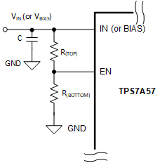
The precision enable circuit (EN pin) turns the device on and off. This circuit can be used to set an external undervoltage lockout (UVLO) voltage, as shown in Figure 8-1, to turn on and off the device using a resistor divider between IN (or BIAS when the charge pump is disabled), EN, and GND.
 Figure 8-1 Precision EN Used as an
External UVLO
Figure 8-1 Precision EN Used as an
External UVLOThis external UVLO solution is used to prevent the device from turning on when the input supply voltage is not high enough and can place the device in dropout operation. This solution also allows simple sequencing of multiple power supplies with a resistor divider from another supply. Another benefit from using a resistor divider to enable or disable the device is that the EN pin is never left floating because this pin does not have an internal pulldown resistor. However, a zener diode may be needed between the EN pin and ground to comply with the absolute maximum ratings on this pin.
Use Equation 1 and Equation 2 to determine the correct resistor values.
where:
- VOFF is the input or bias voltage where the regulator turns off
- VON is the input or bias voltage where the regulator turns on