ZHCSAM1F December   2012  – December 2017 TPS7A66-Q1 , TPS7A69-Q1

PRODUCTION DATA.  

  1. 特性
  2. 应用
  3. 说明
    1.     Device Images
      1.      硬件启用选项
      2.      输入电压感测选项
  4. 修订历史记录
  5. Pin Configuration and Functions
    1.     Pin Functions
  6. Specifications
    1. 6.1 Absolute Maximum Ratings
    2. 6.2 ESD Ratings
    3. 6.3 Recommended Operating Conditions
    4. 6.4 Thermal Information
    5. 6.5 Electrical Characteristics
    6. 6.6 Switching Characteristics
    7. 6.7 Typical Characteristics
  7. Detailed Description
    1. 7.1 Overview
    2. 7.2 Functional Block Diagrams
    3. 7.3 Feature Description
      1. 7.3.1 Enable (EN)
      2. 7.3.2 Regulated Output (VOUT)
      3. 7.3.3 Power-On Reset (PG)
      4. 7.3.4 Reset Delay Timer (CT)
      5. 7.3.5 Sense Comparator (SI and SO for TPS7A69-Q1)
      6. 7.3.6 Adjustable Output Voltage (FB for TPS7A6601-Q1)
      7. 7.3.7 Undervoltage Shutdown
      8. 7.3.8 Low-Voltage Tracking
      9. 7.3.9 Thermal Shutdown
    4. 7.4 Device Functional Modes
      1. 7.4.1 Regulation
      2. 7.4.2 Disabled
      3. 7.4.3 Operation With V(VinUVLO)< VIN < VIN(min)
  8. Application and Implementation
    1. 8.1 Application Information
    2. 8.2 Typical Applications
      1. 8.2.1 TPS7A66-Q1 Typical Application
        1. 8.2.1.1 Design Requirements
        2. 8.2.1.2 Detailed Design Procedure
          1. 8.2.1.2.1 Input Capacitor
          2. 8.2.1.2.2 Output Capacitor
        3. 8.2.1.3 Application Curve
      2. 8.2.2 TPS7A69-Q1 Typical Application
        1. 8.2.2.1 Design Requirements
        2. 8.2.2.2 Detailed Design Procedure
          1. 8.2.2.2.1 Low-Voltage Tracking Threshold
        3. 8.2.2.3 Application Curve
  9. Power Supply Recommendations
  10. 10Layout
    1. 10.1 Layout Guidelines
      1. 10.1.1 Package Mounting
      2. 10.1.2 Board Layout Recommendations to Improve PSRR and Noise Performance
    2. 10.2 Layout Examples
    3. 10.3 Power Dissipation and Thermal Considerations
  11. 11器件和文档支持
    1. 11.1 相关链接
    2. 11.2 接收文档更新通知
    3. 11.3 社区资源
    4. 11.4 商标
    5. 11.5 静电放电警告
    6. 11.6 Glossary
  12. 12机械、封装和可订购信息

封装选项

机械数据 (封装 | 引脚)
散热焊盘机械数据 (封装 | 引脚)
订购信息

Pin Configuration and Functions

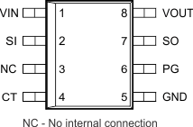
D Package (TPS7A69-Q1)
8-Pin SOIC
Top View
TPS7A66-Q1 TPS7A69-Q1 D-8_PinOut_SLVSBL0.gif
DGN Package (TPS7A66-Q1)
8-Pin HVSSOP
Top View
TPS7A66-Q1 TPS7A69-Q1 DGN-8_PinOut_SLVSBL0.gif

Pin Functions

PIN NAME PIN NO. TYPE DESCRIPTION
SOIC-D HVSSOP-DGN
CT 4 4 O Reset-pulse delay adjustment. Connecting a capacitor from this pin to GND changes the PG reset delay; see the Reset Delay Timer (CT) section for more details.
EN 2 I Enable pin. The device enters the standby state when the enable pin becomes lower than the enable threshold.
FB/DNC 7 I Feedback pin when using external resistor divider or DNC pin when using the device with a fixed output voltage.
GND 5 5 G Ground reference
NC 3 3 Not-connected pin
PG 6 6 O Power good. This open-drain pin must connect to VOUT via an external resistor. VPG is logic level high when VOUT is above the power-on-reset threshold.
SI 2 I Sense input pin to supervise input voltage. Connect via an external voltage divider to VIN and GND.
SO 7 O Sense output. This open-drain pin must connect to VOUT via an external resistor. VSO is logic level low when VSI falls below the sense-low threshold.
VIN 1 1 P Input power-supply voltage
VOUT 8 8 O Regulated output voltage
Thermal pad Pad Thermal pad for HVSSOP-DGN package