ZHCSBT7D May 2013 – April 2017 TPS7A7002
PRODUCTION DATA.
10 Layout
10.1 Layout Guidelines
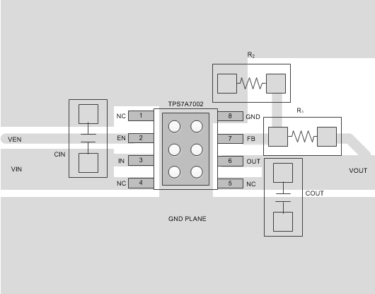
For best performance, place all circuit components on the same side of the circuit board, and place the external components as close to the device as practically possible. The use of vias and long traces is strongly discouraged because of parasitics that might affect performance; follow these guidelines to minimize parasitics. Also, embed a ground reference plane to maintain accuracy of the output voltage and shield noise. Make sure that this plane is connected to the PowerPAD in order to help spread (or sink) heat from the device; be aware that NC pins might be connected to this plane. The recommended layout is shown in Figure 10.
10.2 Layout Example
 Figure 10. Layout Recommendation
10.3 Thermal Consideration
Thermal protection disables the output when the junction temperature rises to approximately 160°C, allowing the device to cool. When the junction temperature cools to approximately 140°C, the output circuitry is re-enabled.
The internal protection circuitry of the TPS7A7002 is designed to protect against overload conditions. The protection circuitry is not intended to replace proper heat sinking. Continuously running the TPS7A7002 into thermal shutdown degrades device reliability.
10.4 Power Dissipation
Power dissipation (PD) of the device depends on the input voltage and load conditions, and is calculated using Equation 3.

In order to minimize power dissipation and achieve greater efficiency, use the lowest possible input voltage necessary to achieve the required output voltage regulation
On the SOIC (DDA) package, the primary conduction path for heat is through the exposed pad to the PCB. The pad can either be connected to ground or left floating; however, attach the pad to an appropriate amount of copper PCB area to prevent the device from overheating. The maximum junction-to-ambient thermal resistance depends on the maximum ambient temperature, maximum device junction temperature, and power dissipation of the device, and is calculated using Equation 4:
