ZHCSBT7D May 2013 – April 2017 TPS7A7002
PRODUCTION DATA.
6 Specifications
6.1 Absolute Maximum Ratings
over junction temperature range (unless otherwise noted)(1)| MIN | MAX | UNIT | ||
|---|---|---|---|---|
| Voltage | IN | –0.3 | 7 | V |
| EN, FB, OUT | –0.3 | VIN + 0.3(2) | ||
| Current | OUT | Internally limited | A | |
| Temperature | Operating virtual junction, TJ | –55 | 150 | °C |
| Storage temperature, Tstg | –55 | 150 | ||
(1) Stresses beyond those listed under Absolute Maximum Ratings may cause permanent damage to the device. These are stress ratings only, which do not imply functional operation of the device at these or any other conditions beyond those indicated under Recommended Operating Conditions. Exposure to absolute-maximum-rated conditions for extended periods may affect device reliability.
(2) The absolute maximum rating is VIN + 0.3 V or 7 V, whichever is smaller.
6.2 ESD Ratings
| VALUE | UNIT | |||
|---|---|---|---|---|
| V(ESD) | Electrostatic discharge | Human body model (HBM), per ANSI/ESDA/JEDEC JS-001(1) | ±2000 | V |
| Charged-device model (CDM), per JEDEC specification JESD22-C101(2) | ±500 | |||
(1) JEDEC document JEP155 states that 500-V HBM allows safe manufacturing with a standard ESD control process.
(2) JEDEC document JEP157 states that 250-V CDM allows safe manufacturing with a standard ESD control process.
6.3 Recommended Operating Conditions
| MIN | NOM | MAX | UNIT | ||
|---|---|---|---|---|---|
| VIN | Input voltage | 1.425 | 6.5 | V | |
| VEN | Enable pin voltage | 0 | VIN | V | |
| CIN | Input capacitor | 1 | 10 | µF | |
| COUT | Output capacitor(1)(2) | 4.7 | 10 | 200 | µF |
| CFB | Feedforward capacitance | 0 | 100 | nF | |
| IOUT | Output current | 0 | 3 | A | |
| TJ | Junction temperature | –40 | 125 | °C | |
(2) For output capacitors larger than 47 µF, a feedforward capacitor of at least 220 pF must be used.
6.4 Thermal Information
| THERMAL METRIC(1) | TPS7A7002 | UNIT | |
|---|---|---|---|
| DDA (SO PowerPAD) | |||
| 8 PINS | |||
| RθJA | Junction-to-ambient thermal resistance | 46.4 | °C/W |
| RθJC(top) | Junction-to-case (top) thermal resistance | 54.2 | °C/W |
| RθJB | Junction-to-board thermal resistance | 29.9 | °C/W |
| ψJT | Junction-to-top characterization parameter | 10.2 | °C/W |
| ψJB | Junction-to-board characterization parameter | 29.8 | °C/W |
| RθJC(bot) | Junction-to-case (bottom) thermal resistance | 6.8 | °C/W |
(1) For more information about traditional and new thermal metrics, see the Semiconductor and IC Package Thermal Metrics application report.
6.5 Electrical Characteristics
Over the full operating temperature range (see Recommended Operating Conditions), VEN = 1.1 V, VFB = VOUT(1), 1.425 V ≤ VIN ≤ 6.5 V, 10 µA ≤ IOUT ≤ 3 A, COUT = 10 μF (unless otherwise noted). Typical values are at TJ = 25°C.| PARAMETER | TEST CONDITIONS | MIN | TYP | MAX | UNIT | ||
|---|---|---|---|---|---|---|---|
| INPUT VOLTAGE | |||||||
| IGND | GND pin current | VIN = 3.3 V, 50-Ω load resistor between OUT and GND |
3 | mA | |||
| Shutdown GND pin current | VIN = 6.5 V, VEN = 0 V | 5 | µA | ||||
| OUTPUT VOLTAGE | |||||||
| VOUT | Output voltage accuracy(2)(3) | VIN = VOUT + 0.5 V(4), IOUT = 10 mA | –2% | 2% | |||
| VIN = 1.8 V, IOUT = 0.8 A, 0°C ≤ TJ = TA ≤ 85°C | –2% | 2% | |||||
| IOUT = 10 mA | –3% | 3% | |||||
| ΔVO(ΔVI) | Line regulation | IOUT = 10 mA | 0.2 | 0.4 | %/V | ||
| ΔVO(ΔIO) | Load regulation(3) | 10 mA ≤ IOUT ≤ 3 A | 0.25 | 0.75 | %/A | ||
| VDO | Dropout voltage (5) | IOUT = 1 A, 0.5 V ≤ VOUT ≤ 5 V | 200 | mV | |||
| IOUT = 2 A, 0.5 V ≤ VOUT ≤ 5 V | 380 | ||||||
| IOUT = 3 A, 0.5 V ≤ VOUT ≤ 4.8 V | 600 | ||||||
| ICL | Output current limit | VIN = 1.425 V, VOUT = 0.9 × VOUT(NOM) | 3.36 | A | |||
| FEEDBACK | |||||||
| VREF | Reference voltage accuracy | VIN = 3.3 V, IOUT = 10 mA | 0.49 | 0.5 | 0.51 | V | |
| IFB | FB pin current | VFB = 0.5 V | 1 | µA | |||
| ENABLE | |||||||
| IEN | EN pin current | VEN = 0 V, VIN = 3.3 V | 0.2 | µA | |||
| VEN(LO) | EN pin input low (disable) | VIN = 3.3 V | 0 | 0.5 | V | ||
| VEN(HI) | EN pin input high (enable) | VIN = 3.3 V | 1.1 | VIN | V | ||
| TEMPERATURE | |||||||
| TSD | Thermal shutdown temperature | Shutdown, temperature increasing | 160 | °C | |||
| Reset, temperature decreasing | 140 | ||||||
(1) When setting VOUT to a value other than 0.5 V, connect R2 to the FB pin using 27-kΩ ≤ R2 ≤ 33-kΩ resistors. See Figure 7 for details of R1 and R2.
(2) Accuracy does not include error on feedback resistors R1 and R2.
(3) TPS7A7002 is not tested at VOUT = 0.5 V, 2.3 V ≤ VIN ≤ 6.5 V, and 500 mA ≤ IOUT ≤ 3 A because the power dissipation is higher than the maximum rating of the package. Also, this accuracy specification does not apply to any application condition that exceeds the power dissipation limit of the package.
(4) VIN = VOUT + 0.5 V or 1.425 V, whichever is greater.
(5) VDO = VIN – VOUT with VFB = GND configuration.
6.6 Typical Characteristics
for all fixed voltage versions and an adjustable version at TJ = 25°C, VEN = VIN, CIN = 10 μF, COUT = 10 μF, and using the component values in Table 2 (unless otherwise noted)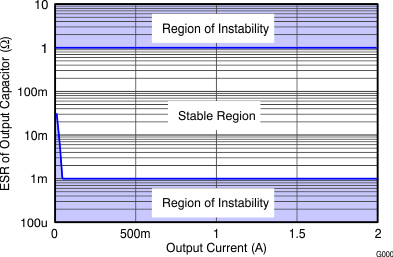
| COUT = 10 µF |
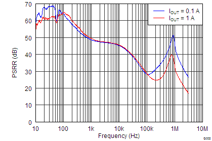
| VIN = 5 V, VOUT = 3.3 V |
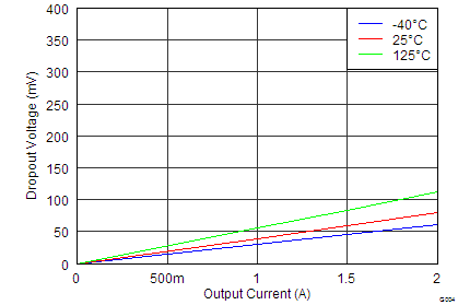
| VOUT = 1.6 V |
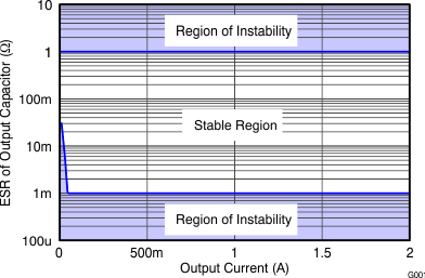
| COUT = 100 µF |
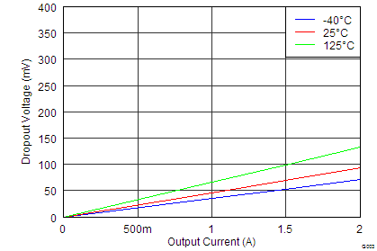
| VOUT = 3.3 V |
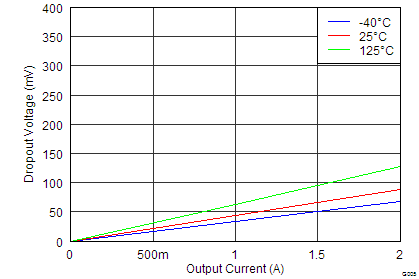
| VOUT = 1.4 V |