ZHCS837F March 2012 – October 2023 TPS7A7300
PRODUCTION DATA
- 1
- 1 特性
- 2 应用
- 3 说明
- 4 Pin Configurations
- 5 Specifications
- 6 Detailed Description
- 7 Application and Implementation
- 8 Device And Documentation Support
- 9 Revision History
- 10Mechanical, Packaging, And Orderable Information
6.3.1 User-Configurable Output Voltage
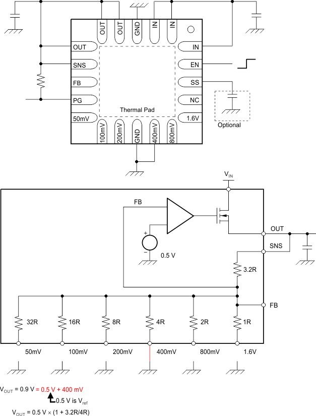
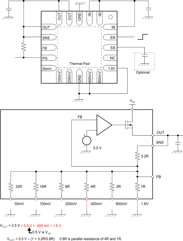
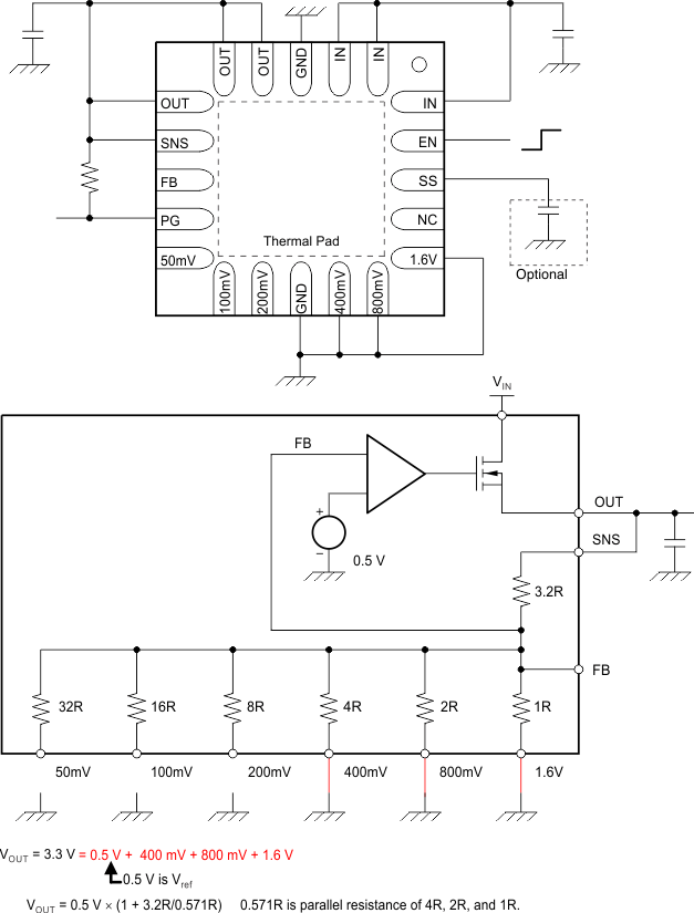
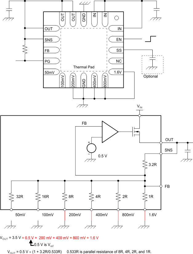
Unlike traditional LDO devices, the TPS7A7300 comes with only one orderable part number. There is no adjustable or fixed output voltage option. The output voltage of the TPS7A7300 is selectable in accordance with the names given to the output voltage setting pins: 50 mV, 100 mV, 200 mV, 400 mV, 800 mV, and 1.6 V. For each pin connected to the ground, the output voltage setting increases by the value associated with that pin name, starting from the value of the reference voltage of 0.5 V. Floating the pins has no effect on the output voltage. Figure 6-1 through Figure 6-6 show examples of how to program the output voltages.
 Figure 6-1 0.9-V Configuration
 Figure 6-2 1.2-V Configuration
 Figure 6-3 1.8-V Configuration
 Figure 6-4 2.5-V Configuration
 Figure 6-5 3.3-V Configuration
 Figure 6-6 3.5-V Configuration
See Table 6-1 for a full list of target output voltages and corresponding pin settings. The voltage setting pins have a binary weight; therefore, the output voltage can be programmed to any value from 0.9 V to 3.5 V in 50-mV steps.
Figure 5-11 and Figure 5-12 illustrate this output voltage programming performance.
Any output voltage setting that is not listed in Table 6-1 is not covered in the Electrical Characteristics . For output voltages greater than 3.5 V, use a traditional adjustable configuration (see the Traditional Adjustable ConfigurationTraditional Adjustable ConfigurationTraditional Adjustable Configuration section).
| VOUT(TARGET) (V) |
50 mV | 100 mV | 200 mV | 400 mV | 800 mV | 1.6 V |
|---|---|---|---|---|---|---|
| 0.9 | open | open | open | GND | open | open |
| 0.95 | GND | open | open | GND | open | open |
| 1 | open | GND | open | GND | open | open |
| 1.05 | GND | GND | open | GND | open | open |
| 1.1 | open | open | GND | GND | open | open |
| 1.15 | GND | open | GND | GND | open | open |
| 1.2 | open | GND | GND | GND | open | open |
| 1.25 | GND | GND | GND | GND | open | open |
| 1.3 | open | open | open | open | GND | open |
| 1.35 | GND | open | open | open | GND | open |
| 1.4 | open | GND | open | open | GND | open |
| 1.45 | GND | GND | open | open | GND | open |
| 1.5 | open | open | GND | open | GND | open |
| 1.55 | GND | open | GND | open | GND | open |
| 1.6 | open | GND | GND | open | GND | open |
| 1.65 | GND | GND | GND | open | GND | open |
| 1.7 | open | open | open | GND | GND | open |
| 1.75 | GND | open | open | GND | GND | open |
| 1.8 | open | GND | open | GND | GND | open |
| 1.85 | GND | GND | open | GND | GND | open |
| 1.9 | open | open | GND | GND | GND | open |
| 1.95 | GND | open | GND | GND | GND | open |
| 2 | open | GND | GND | GND | GND | open |
| 2.05 | GND | GND | GND | GND | GND | open |
| 2.1 | open | open | open | open | open | GND |
| 2.15 | GND | open | open | open | open | GND |
| 2.2 | open | GND | open | open | open | GND |
| 2.25 | GND | GND | open | open | open | GND |
| 2.3 | open | open | GND | open | open | GND |
| 2.35 | GND | open | GND | open | open | GND |
| 2.4 | open | GND | GND | open | open | GND |
| 2.45 | GND | GND | GND | open | open | GND |
| 2.5 | open | open | open | GND | open | GND |
| 2.55 | GND | open | open | GND | open | GND |
| 2.6 | open | GND | open | GND | open | GND |
| 2.65 | GND | GND | open | GND | open | GND |
| 2.7 | open | open | GND | GND | open | GND |
| 2.75 | GND | open | GND | GND | open | GND |
| 2.8 | open | GND | GND | GND | open | GND |
| 2.85 | GND | GND | GND | GND | open | GND |
| 2.9 | open | open | open | open | GND | GND |
| 2.95 | GND | open | open | open | GND | GND |
| 3 | open | GND | open | open | GND | GND |
| 3.05 | GND | GND | open | open | GND | GND |
| 3.1 | open | open | GND | open | GND | GND |
| 3.15 | GND | open | GND | open | GND | GND |
| 3.2 | open | GND | GND | open | GND | GND |
| 3.25 | GND | GND | GND | open | GND | GND |
| 3.3 | open | open | open | GND | GND | GND |
| 3.35 | GND | open | open | GND | GND | GND |
| 3.4 | open | GND | open | GND | GND | GND |
| 3.45 | GND | GND | open | GND | GND | GND |
| 3.5 | open | open | GND | GND | GND | GND |