ZHCSO39B May 2022 – August 2022 TPS7A74
PRODUCTION DATA
- 1 特性
- 2 应用
- 3 说明
- 4 Revision History
- 5 Pin Configuration and Functions
- 6 Specifications
- 7 Detailed Description
- 8 Application and Implementation
- 9 Device and Documentation Support
- 10Mechanical, Packaging, and Orderable Information
7.3.4 Internal Current Limit
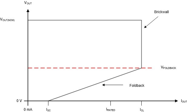
The device has an internal current-limit circuit that protects the regulator during transient high-load current faults or shorting events. The current limit is a hybrid brick-wall foldback scheme. The current limit transitions from a brick-wall scheme to a foldback scheme at the foldback voltage (VFOLDBACK). In a high-load current fault with the output voltage above VFOLDBACK, the brick-wall scheme limits the output current to the current limit (ICL). When the voltage drops below VFOLDBACK, a foldback current limit activates that scales back the current when the output voltage approaches GND. When the output is shorted, the device supplies a typical current called the short-circuit current limit (ISC). ICL and ISC are listed in the Section 6.5 table.
For this device, VFOLDBACK is approximately 60% × VOUT(nom).
The output voltage is not regulated when the device is in current limit. When a current-limit event occurs, the device begins to heat up because of the increase in power dissipation. When the device is in a brick-wall current limit, the pass transistor dissipates power [(VIN – VOUT) × ICL]. When the device output is shorted and the output is below VFOLDBACK, the pass transistor dissipates power [(VIN – VOUT) × ISC]. If thermal shutdown is triggered, the device turns off. When the device sufficiently cools down, the internal thermal shutdown circuit turns the device back on. If the output current fault condition continues, the device cycles between current limit and thermal shutdown. For more information on current limits, see the Know Your Limits application note. Figure 7-2 illustrates a diagram of the foldback current limit.
 Figure 7-2 Foldback Current
Limit