ZHCSJG2A March 2019 – September 2019 TPS7A78
PRODUCTION DATA.
- 1 特性
- 2 应用
- 3 说明
- 4 修订历史记录
- 5 Pin Configuration and Functions
- 6 Specifications
-
7 Detailed Description
- 7.1 Overview
- 7.2 Functional Block Diagram
- 7.3
Feature Description
- 7.3.1 Active Bridge Control
- 7.3.2 Full-Bridge (FB) and Half-Bridge (HB) Configurations
- 7.3.3 4:1 Switched-Capacitor Voltage Reduction
- 7.3.4 Undervoltage Lockout Circuits (VUVLO_SCIN) and (VUVLO_LDO_IN)
- 7.3.5 Dropout Voltage Regulation
- 7.3.6 Current Limit
- 7.3.7 Programmable Power-Fail Detection
- 7.3.8 Power-Good (PG) Detection
- 7.3.9 Thermal Shutdown
- 7.4 Device Functional Modes
-
8 Application and Implementation
- 8.1
Application Information
- 8.1.1 Recommended Capacitor Types
- 8.1.2 Input and Output Capacitors Requirements
- 8.1.3 Startup Behavior
- 8.1.4 Load Transient
- 8.1.5 Standby Power and Output Efficiency
- 8.1.6 Reverse Current
- 8.1.7 Switched-Capacitor Stage Output Impedance
- 8.1.8 Power Dissipation (PD)
- 8.1.9 Estimating Junction Temperature
- 8.2
Typical Application
- 8.2.1 Design Requirements
- 8.2.2
Detailed Design Procedure
- 8.2.2.1 Calculating the Cap-Drop Capacitor CS
- 8.2.2.2 Calculating the Surge Resistor RS
- 8.2.2.3 Checking for the Device Maximum ISHUNT Current
- 8.2.2.4 Calculating the Bulk Capacitor CSCIN
- 8.2.2.5 Calculating the PFD Pin Resistor Dividers for a Power-Fail Detection
- 8.2.2.6 Summary of the Typical Application Design Components
- 8.2.3 Application Curves
- 8.1
Application Information
- 9 Power Supply Recommendations
- 10Layout
- 11器件和文档支持
- 12机械、封装和可订购信息
8.1.4 Load Transient
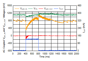
A load-transient event can trigger the internal overcharge protection circuit on the LDO_IN pin. This condition prevents CLDO_IN from overcharging when a heavy load is abruptly removed. The overvoltage protection circuit engages and prevents the switched capacitors from switching until the excess charge on CLDO_IN is discharged into the load. This protection behavior occurs most often during heavy load-transient events on devices with higher output voltages. The value of the CLDO_IN capacitor and the load current determine how long the overvoltage protection circuit remains engaged. Figure 21 shows the overvoltage protection circuit behavior after the load is removed without tripping the PG signal.
 Figure 21. Overvoltage Protection Circuit Behavior for a 5.0-V Output Voltage Device During Load Transient
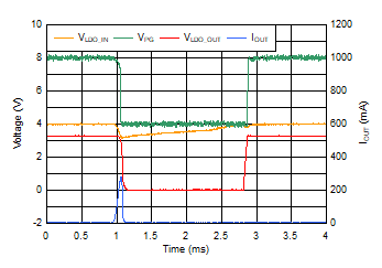
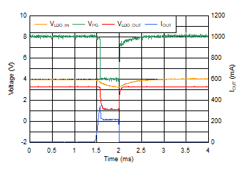
 As illustrated in Figure 22, a load-transient event that exceeds the maximum output current can disable the output when the heavy load pulls down the VLDO_IN voltage below the VUVLO_LDO_IN falling threshold. If the application is prone to heavy load-transient events as illustrated in Figure 22, increase the CLDO_IN capacitor value as necessary. However, as illustrated in Figure 20, too large of a CLDO_IN leads to a longer startup time.

| VAC = 120 VRMS at 60 Hz, FB, CLDO_IN = 10 µF,
VLDO_OUT = 3.3 V, IOUT = 1 mA to 600 mA, current slew = 1 A/µs |

| VAC = 120 VRMS at 60 Hz, FB, CLDO_IN = 56 µF,
VLDO_OUT = 3.3 V, IOUT = 1 mA to 600 mA, current slew = 1 A/µs |
||