ZHCSJG2A March 2019 – September 2019 TPS7A78
PRODUCTION DATA.
- 1 特性
- 2 应用
- 3 说明
- 4 修订历史记录
- 5 Pin Configuration and Functions
- 6 Specifications
-
7 Detailed Description
- 7.1 Overview
- 7.2 Functional Block Diagram
- 7.3
Feature Description
- 7.3.1 Active Bridge Control
- 7.3.2 Full-Bridge (FB) and Half-Bridge (HB) Configurations
- 7.3.3 4:1 Switched-Capacitor Voltage Reduction
- 7.3.4 Undervoltage Lockout Circuits (VUVLO_SCIN) and (VUVLO_LDO_IN)
- 7.3.5 Dropout Voltage Regulation
- 7.3.6 Current Limit
- 7.3.7 Programmable Power-Fail Detection
- 7.3.8 Power-Good (PG) Detection
- 7.3.9 Thermal Shutdown
- 7.4 Device Functional Modes
-
8 Application and Implementation
- 8.1
Application Information
- 8.1.1 Recommended Capacitor Types
- 8.1.2 Input and Output Capacitors Requirements
- 8.1.3 Startup Behavior
- 8.1.4 Load Transient
- 8.1.5 Standby Power and Output Efficiency
- 8.1.6 Reverse Current
- 8.1.7 Switched-Capacitor Stage Output Impedance
- 8.1.8 Power Dissipation (PD)
- 8.1.9 Estimating Junction Temperature
- 8.2
Typical Application
- 8.2.1 Design Requirements
- 8.2.2
Detailed Design Procedure
- 8.2.2.1 Calculating the Cap-Drop Capacitor CS
- 8.2.2.2 Calculating the Surge Resistor RS
- 8.2.2.3 Checking for the Device Maximum ISHUNT Current
- 8.2.2.4 Calculating the Bulk Capacitor CSCIN
- 8.2.2.5 Calculating the PFD Pin Resistor Dividers for a Power-Fail Detection
- 8.2.2.6 Summary of the Typical Application Design Components
- 8.2.3 Application Curves
- 8.1
Application Information
- 9 Power Supply Recommendations
- 10Layout
- 11器件和文档支持
- 12机械、封装和可订购信息
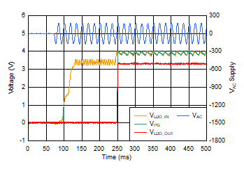
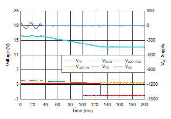
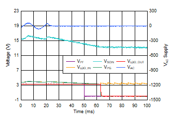
8.2.3 Application Curves

| CS = 330 nF, CSCIN = 47 µF, CSC1 = CSC2 = 1.0 µF,
CLDO_IN = CLDO_OUT = 1.0 µF, IOUT = 12 mA |

| CS = 330 nF, CSCIN = 120 µF, CSC1 = CSC2 = 1.0 µF,
CLDO_IN = CLDO_OUT = 1.0 µF, IOUT = 12 mA |

| CS = 330 nF, CSCIN = 47 µF, CSC1 = CSC2 = 1.0 µF,
CLDO_IN = CLDO_OUT = 1.0 µF, IOUT = 12 mA |