ZHCSH45B June 2017 – October 2021 TPS7A83A
PRODUCTION DATA
- 1 特性
- 2 应用
- 3 说明
- 4 Revision History
- 5 说明(续)
- 6 Pin Configuration and Functions
-
7 Specifications
- 7.1 Absolute Maximum Ratings
- 7.2 ESD Ratings
- 7.3 Recommended Operating Conditions
- 7.4 Thermal Information
- 7.5 Electrical Characteristics: General
- 7.6 Electrical Characteristics: TPS7A8300A
- 7.7 Electrical Characteristics: TPS7A8301A
- 7.8 Typical Characteristics: TPS7A8300A
- 7.9 Typical Characteristics: TPS7A8301A
- 8 Detailed Description
-
9 Application and Implementation
- 9.1
Application Information
- 9.1.1
External Component Selection
- 9.1.1.1 Adjustable Operation
- 9.1.1.2 ANY-OUT Programmable Output Voltage
- 9.1.1.3 ANY-OUT Operation
- 9.1.1.4 Increasing ANY-OUT Resolution for LILO Conditions
- 9.1.1.5 Recommended Capacitor Types
- 9.1.1.6 Input and Output Capacitor Requirements (CIN and COUT)
- 9.1.1.7 Feed-Forward Capacitor (CFF)
- 9.1.1.8 Noise-Reduction and Soft-Start Capacitor (CNR/SS)
- 9.1.2 Start Up
- 9.1.3 AC and Transient Performance
- 9.1.4 DC Performance
- 9.1.5 Sequencing Requirements
- 9.1.6 Negatively Biased Output
- 9.1.7 Reverse Current
- 9.1.8 Power Dissipation (PD)
- 9.1.1
External Component Selection
- 9.2 Typical Application
- 9.1
Application Information
- 10Power Supply Recommendations
- 11Layout
- 12Device and Documentation Support
- 13Mechanical, Packaging, and Orderable Information
封装选项
机械数据 (封装 | 引脚)
散热焊盘机械数据 (封装 | 引脚)
订购信息
9.1.2.2 Undervoltage Lockout (UVLO)
The UVLO circuits ensure that the device stays disabled before the input or bias supplies reach the minimum operational voltage range, and ensures that the device properly shuts down when either the input or BIAS supply collapses.
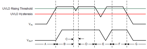
Figure 9-4 and Table 9-5 show one of the UVLO circuits being triggered to various input voltage events, assuming VEN ≥ VIH(EN).
 Figure 9-4 Typical UVLO Operation
| REGION | EVENT | VOUT STATUS | COMMENT |
|---|---|---|---|
| A | Turn on, VIN ≥ VUVLO_1,2(IN), and VBIAS ≥ VUVLO(BIAS) | Off | Start up |
| B | Regulation | On | Regulates to target VOUT |
| C | Brownout, VIN ≥
VUVLO_1,2(IN) – VHYS_1,2(IN)
or VBIAS ≥ VUVLO(BIAS) – VHYS(BIAS) |
On | The output can fall out of regulation but the device is still enabled |
| D | Regulation | On | Regulates to target VOUT |
| E | Brownout, VIN <
VUVLO_1,2(IN) – VHYS_1,2(IN) or VBIAS ≥ VUVLO(BIAS) – VHYS(BIAS) |
Off | The device is disabled and the output falls because of the load and active discharge circuit. The device is re-enabled when the UVLO fault is removed when either the IN or BIAS UVLO rising threshold is reached by the input or bias voltage and a normal start up then follows. |
| F | Regulation | On | Regulates to target VOUT |
| G | Turn off, VIN <
VUVLO_1,2(IN) – VHYS_1,2(IN) or VBIAS < VUVLO(BIAS) – VHYS(BIAS) |
Off | The output falls because of the load and active discharge circuit |
Similar to many other LDOs with this feature, the UVLO circuits take a few microseconds to fully assert. During this time, a downward line transient below approximately 0.8 V causes the UVLO to assert for a short time; however, the UVLO circuits do not have enough stored energy to fully discharge the internal circuits inside the device. When the UVLO circuits are not given enough time to fully discharge the internal nodes, the outputs are not fully disabled.
The effect of the downward line transient can be mitigated by using a larger input capacitor to increase the fall time of the input supply when operating near the minimum VIN.