ZHCSH45B June 2017 – October 2021 TPS7A83A
PRODUCTION DATA
- 1 特性
- 2 应用
- 3 说明
- 4 Revision History
- 5 说明(续)
- 6 Pin Configuration and Functions
-
7 Specifications
- 7.1 Absolute Maximum Ratings
- 7.2 ESD Ratings
- 7.3 Recommended Operating Conditions
- 7.4 Thermal Information
- 7.5 Electrical Characteristics: General
- 7.6 Electrical Characteristics: TPS7A8300A
- 7.7 Electrical Characteristics: TPS7A8301A
- 7.8 Typical Characteristics: TPS7A8300A
- 7.9 Typical Characteristics: TPS7A8301A
- 8 Detailed Description
-
9 Application and Implementation
- 9.1
Application Information
- 9.1.1
External Component Selection
- 9.1.1.1 Adjustable Operation
- 9.1.1.2 ANY-OUT Programmable Output Voltage
- 9.1.1.3 ANY-OUT Operation
- 9.1.1.4 Increasing ANY-OUT Resolution for LILO Conditions
- 9.1.1.5 Recommended Capacitor Types
- 9.1.1.6 Input and Output Capacitor Requirements (CIN and COUT)
- 9.1.1.7 Feed-Forward Capacitor (CFF)
- 9.1.1.8 Noise-Reduction and Soft-Start Capacitor (CNR/SS)
- 9.1.2 Start Up
- 9.1.3 AC and Transient Performance
- 9.1.4 DC Performance
- 9.1.5 Sequencing Requirements
- 9.1.6 Negatively Biased Output
- 9.1.7 Reverse Current
- 9.1.8 Power Dissipation (PD)
- 9.1.1
External Component Selection
- 9.2 Typical Application
- 9.1
Application Information
- 10Power Supply Recommendations
- 11Layout
- 12Device and Documentation Support
- 13Mechanical, Packaging, and Orderable Information
封装选项
机械数据 (封装 | 引脚)
散热焊盘机械数据 (封装 | 引脚)
订购信息
8.3.1.1 DC Regulation
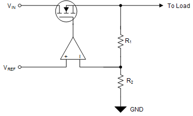
As Figure 8-1 shows, an LDO functions as a class-B amplifier in which the input signal is the internal reference voltage (VREF). VREF is designed to have a very low bandwidth at the input to the error amplifier through the use of a low-pass filter (VNR/SS).
As such, the reference can be considered as a pure dc input signal. The low output impedance of an LDO comes from the combination of the output capacitor and pass element. The pass element also presents a high input impedance to the source voltage when operating as a current source. A positive LDO can only source current because of the class-B architecture.
This device achieves a maximum of 0.75% output voltage accuracy primarily because of the high-precision band-gap voltage (VBG) that creates VREF. The low dropout voltage (VDO) reduces the thermal power dissipation required by the device to regulate the output voltage at a given current level, thereby improving system efficiency. These features combine to make this device a good approximation of an ideal voltage source.
