ZHCSH45B June 2017 – October 2021 TPS7A83A
PRODUCTION DATA
- 1 特性
- 2 应用
- 3 说明
- 4 Revision History
- 5 说明(续)
- 6 Pin Configuration and Functions
-
7 Specifications
- 7.1 Absolute Maximum Ratings
- 7.2 ESD Ratings
- 7.3 Recommended Operating Conditions
- 7.4 Thermal Information
- 7.5 Electrical Characteristics: General
- 7.6 Electrical Characteristics: TPS7A8300A
- 7.7 Electrical Characteristics: TPS7A8301A
- 7.8 Typical Characteristics: TPS7A8300A
- 7.9 Typical Characteristics: TPS7A8301A
- 8 Detailed Description
-
9 Application and Implementation
- 9.1
Application Information
- 9.1.1
External Component Selection
- 9.1.1.1 Adjustable Operation
- 9.1.1.2 ANY-OUT Programmable Output Voltage
- 9.1.1.3 ANY-OUT Operation
- 9.1.1.4 Increasing ANY-OUT Resolution for LILO Conditions
- 9.1.1.5 Recommended Capacitor Types
- 9.1.1.6 Input and Output Capacitor Requirements (CIN and COUT)
- 9.1.1.7 Feed-Forward Capacitor (CFF)
- 9.1.1.8 Noise-Reduction and Soft-Start Capacitor (CNR/SS)
- 9.1.2 Start Up
- 9.1.3 AC and Transient Performance
- 9.1.4 DC Performance
- 9.1.5 Sequencing Requirements
- 9.1.6 Negatively Biased Output
- 9.1.7 Reverse Current
- 9.1.8 Power Dissipation (PD)
- 9.1.1
External Component Selection
- 9.2 Typical Application
- 9.1
Application Information
- 10Power Supply Recommendations
- 11Layout
- 12Device and Documentation Support
- 13Mechanical, Packaging, and Orderable Information
封装选项
机械数据 (封装 | 引脚)
散热焊盘机械数据 (封装 | 引脚)
订购信息
9.1.3.4 Load Transient Response
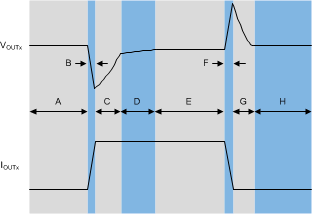
The load-step transient response is the output voltage response by the LDO to a step in load current, whereby output voltage regulation is maintained. There are two key transitions during a load transient response: the transition from a light to a heavy load and the transition from a heavy to a light load. The regions shown in Figure 9-9 and described in Table 9-9 are broken down in this section. Regions A, E, and H are where the output voltage is in steady-state.
 Figure 9-9 Load Transient Waveform
| REGION | DESCRIPTION | COMMENT |
|---|---|---|
| A | Regulation | Regulation |
| B | Output current ramping | Initial voltage dip is a result of the depletion of the output capacitor charge |
| C | LDO responding to transient | Recovery from the dip results from the LDO increasing its sourcing current, and leads to output voltage regulation |
| D | Reaching thermal equilibrium | At high load currents the LDO takes some time to heat up. During this time the output voltage changes slightly. |
| E | Regulation | Regulation |
| F | Output current ramping | Initial voltage rise results from the LDO sourcing a large current, and leads to the output capacitor charge to increase |
| G | LDO responding to transient | Recovery from the rise results from the LDO decreasing its sourcing current in combination with the load discharging the output capacitor |
| H | Regulation | Regulation |
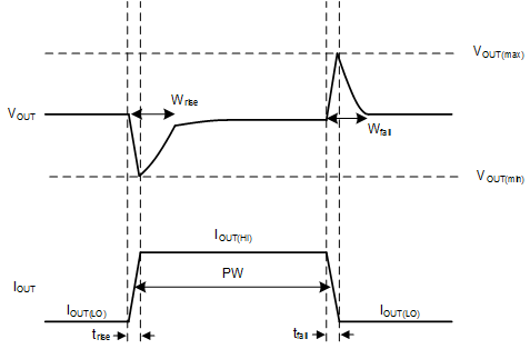
The transient response peaks (VOUT(max) and VOUT(min)) are improved by using more output capacitance; however, doing so slows down the recovery time (Wrise and Wfall). Figure 9-10 shows these parameters during a load transient, with a given pulse duration (PW) and current levels (IOUT(LO) and IOUT(HI)).
 Figure 9-10 Simplified Load Transient Waveform