ZHCSEI2B January 2016 – June 2021 TPS7A84
PRODUCTION DATA
- 1 特性
- 2 应用
- 3 说明
- 4 Revision History
- 5 Pin Configurations and Functions
- 6 Specifications
- 7 Detailed Description
-
8 Application and Implementation
- 8.1
Application Information
- 8.1.1 Recommended Capacitor Types
- 8.1.2 Input and Output Capacitor Requirements (CIN and COUT)
- 8.1.3 Noise-Reduction and Soft-Start Capacitor (CNR/SS)
- 8.1.4 Feed-Forward Capacitor (CFF)
- 8.1.5 Soft-Start and In-Rush Current
- 8.1.6 Optimizing Noise and PSRR
- 8.1.7 Charge Pump Noise
- 8.1.8 ANY-OUT Programmable Output Voltage
- 8.1.9 ANY-OUT Operation
- 8.1.10 Increasing ANY-OUT Resolution for LILO Conditions
- 8.1.11 Current Sharing
- 8.1.12 Adjustable Operation
- 8.1.13 Sequencing Requirements
- 8.1.14 Power-Good Operation
- 8.1.15 Undervoltage Lockout (UVLO) Operation
- 8.1.16 Dropout Voltage (VDO)
- 8.1.17 Behavior when Transitioning from Dropout into Regulation
- 8.1.18 Load Transient Response
- 8.1.19 Negatively-Biased Output
- 8.1.20 Reverse Current Protection
- 8.1.21 Power Dissipation (PD)
- 8.1.22 Estimating Junction Temperature
- 8.1.23 Recommended Area for Continuous Operation (RACO)
- 8.2 Typical Applications
- 8.1
Application Information
- 9 Power Supply Recommendations
- 10Layout
- 11Device and Documentation Support
- 12Mechanical, Packaging, and Orderable Information
8.1.7 Charge Pump Noise
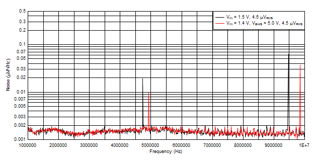
The device internal charge pump generates a minimal amount of noise, as shown in Figure 8-1.
Using a bias rail minimizes the internal charge pump noise when the internal voltage is clamped, thereby reducing the overall output noise floor.
The high-frequency components of the output voltage noise density curve are filtered out in most applications by using 10-nF to 100-nF bypass capacitors close to the load. Using a ferrite bead between the LDO output and the load input capacitors forms a pi-filter, further reducing the high-frequency noise contribution.
 Figure 8-1 Charge Pump Noise