ZHCSEI2B January 2016 – June 2021 TPS7A84
PRODUCTION DATA
- 1 特性
- 2 应用
- 3 说明
- 4 Revision History
- 5 Pin Configurations and Functions
- 6 Specifications
- 7 Detailed Description
-
8 Application and Implementation
- 8.1
Application Information
- 8.1.1 Recommended Capacitor Types
- 8.1.2 Input and Output Capacitor Requirements (CIN and COUT)
- 8.1.3 Noise-Reduction and Soft-Start Capacitor (CNR/SS)
- 8.1.4 Feed-Forward Capacitor (CFF)
- 8.1.5 Soft-Start and In-Rush Current
- 8.1.6 Optimizing Noise and PSRR
- 8.1.7 Charge Pump Noise
- 8.1.8 ANY-OUT Programmable Output Voltage
- 8.1.9 ANY-OUT Operation
- 8.1.10 Increasing ANY-OUT Resolution for LILO Conditions
- 8.1.11 Current Sharing
- 8.1.12 Adjustable Operation
- 8.1.13 Sequencing Requirements
- 8.1.14 Power-Good Operation
- 8.1.15 Undervoltage Lockout (UVLO) Operation
- 8.1.16 Dropout Voltage (VDO)
- 8.1.17 Behavior when Transitioning from Dropout into Regulation
- 8.1.18 Load Transient Response
- 8.1.19 Negatively-Biased Output
- 8.1.20 Reverse Current Protection
- 8.1.21 Power Dissipation (PD)
- 8.1.22 Estimating Junction Temperature
- 8.1.23 Recommended Area for Continuous Operation (RACO)
- 8.2 Typical Applications
- 8.1
Application Information
- 9 Power Supply Recommendations
- 10Layout
- 11Device and Documentation Support
- 12Mechanical, Packaging, and Orderable Information
8.1.19 Negatively-Biased Output
The device does not start or operate as expected if the output voltage is pulled below ground. This issue commonly occurs when powering a split-rail system where the negative rail is established before the device is enabled. Several application solutions are:
- Enable the device before the negative regulator and disable the device after the negative regulator.
- Delaying the EN voltage with respect to the IN voltage allows the internal pulldown resistor to discharge any voltage at OUT. If the discharge circuit is not strong enough to keep the output voltage at ground, then use an external pulldown resistor.
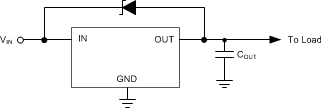
- Place a zener diode from IN to OUT to provide a small positive dc bias on the output when the input is supplied to the device, as shown in Figure 8-10.
 Figure 8-10 Zener Diode Placed from IN to OUT
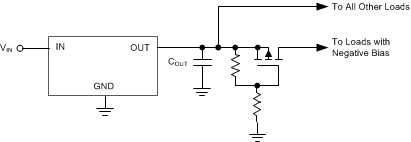
 - Use a PFET to isolate the output of the device from the load causing the negative bias when the device is off, as shown in Figure 8-11.
 Figure 8-11 PFET to Isolate the Output from the Load