ZHCSL68C April 2017 – December 2020 TPS7A84A
PRODUCTION DATA
- 1 特性
- 2 应用
- 3 说明
- 4 Revision History
- 5 Pin Configuration and Functions
-
6 Specifications
- 6.1 Absolute Maximum Ratings
- 6.2 ESD Ratings
- 6.3 Recommended Operating Conditions
- 6.4 Thermal Information
- 6.5 Electrical Characteristics: General
- 6.6 Electrical Characteristics: TPS7A8400A
- 6.7 Electrical Characteristics: TPS7A8401A
- 6.8 Typical Characteristics: TPS7A8400A
- 6.9 Typical Characteristics: TPS7A8401A
- 7 Detailed Description
-
8 Application and Implementation
- 8.1
Application Information
- 8.1.1
External Component Selection
- 8.1.1.1 Adjustable Operation
- 8.1.1.2 ANY-OUT Programmable Output Voltage
- 8.1.1.3 ANY-OUT Operation
- 8.1.1.4 Increasing ANY-OUT Resolution for LILO Conditions
- 8.1.1.5 Current Sharing
- 8.1.1.6 Recommended Capacitor Types
- 8.1.1.7 Input and Output Capacitor Requirements (CIN and COUT)
- 8.1.1.8 Feed-Forward Capacitor (CFF)
- 8.1.1.9 Noise-Reduction and Soft-Start Capacitor (CNR/SS)
- 8.1.2 Start-Up
- 8.1.3 AC and Transient Performance
- 8.1.4 DC Performance
- 8.1.5 Sequencing Requirements
- 8.1.6 Negatively Biased Output
- 8.1.7 Reverse Current Protection
- 8.1.8 Power Dissipation (PD)
- 8.1.1
External Component Selection
- 8.2 Typical Applications
- 8.1
Application Information
- 9 Power Supply Recommendations
- 10Layout
- 11Device and Documentation Support
5 Pin Configuration and Functions
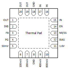
 Figure 5-1
RGR Package (TPS7A8400A),
20-Pin VQFN,
Top View
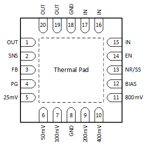
 Figure 5-2
RGR Package (TPS7A8401A),
20-Pin VQFN,
Top View
Table 5-1 Pin Functions
| PIN | TPS7A8400A | TPS7A8401A | I/O | DESCRIPTION |
|---|---|---|---|---|
| 25mV | — | 5 | I | ANY-OUT voltage setting pins. These pins connect to an internal feedback network. Connect these pins to ground, SNS, or leave floating. Connecting these pins to ground increases the output voltage, whereas connecting these pins to SNS increases the resolution of the ANY-OUT network but decreases the range of the network; multiple pins may be simultaneously connected to GND or SNS to select the desired output voltage. Leave these pins floating (open) when not in use. See the Section 8.1.1.2 section for additional details. |
| 50mV | 5 |
6 |
||
| 100mV | 6 |
7 |
||
| 200mV | 7 |
9 |
||
| 400mV | 9 |
10 |
||
| 800mV | 10 | 11 | ||
| 1.6V | 11 | — | ||
| BIAS | 12 | 12 | I | BIAS supply voltage. This pin enables the use of low-input voltage, low-output (LILO) voltage conditions (that is, VIN = 1.2 V, VOUT = 1 V) to reduce power dissipation across the die. The use of a BIAS voltage improves dc and ac performance for VIN ≤ 2.2 V. A 1-µF capacitor (0.47-µF capacitance) or larger must be connected between this pin and ground. If not used, this pin must be left floating or tied to ground. |
| EN | 14 | 14 | I | Enable pin. Driving this pin to logic high enables the device; driving this pin to logic low disables the device. If enable functionality is not required, this pin must be connected to IN or BIAS. |
| FB | 3 | 3 | I | Feedback pin connected to the error amplifier. Although not required, TI recommends a 10-nF feed-forward capacitor from FB to OUT (as close to the device as possible) to maximize ac performance. The use of a feed-forward capacitor may disrupt Power-Good (PG) functionality. See the ANY-OUT Programmable Output Voltage and Section 8.1.1.1 sections for more details. |
| GND | 8, 18 | 8, 18 | — | Ground pin. These pins must be connected to ground, the thermal pad, and each other with a low-impedance connection. |
| IN | 15-17 | 15-17 | I | Input supply voltage pin. A 10-μF or larger ceramic capacitor (5 μF of capacitance or greater) from IN to ground is required to reduce the impedance of the input supply. Place the input capacitor as close as possible to the input. See the Input and Output Capacitor Requirements section for more details. |
| NR/SS | 13 | 13 | — | Noise-reduction and soft-start pin. Connecting an external capacitor between this pin and ground reduces reference voltage noise and also enables the soft-start function. Although not required, TI recommends a 10-nF or larger capacitor be connected from NR/SS to GND (as close as possible to the pin) to maximize ac performance. See the Input and Output Capacitor Requirements section for more details. |
| OUT | 1, 19, 20 | 1, 19, 20 | O | Regulated output pin. A 47-μF or larger ceramic capacitor (25 μF of capacitance or greater) from OUT to ground is required for stability and must be placed as close as possible to the output. Minimize the impedance from the OUT pin to the load. See the Input and Output Capacitor Requirements sections for more details. |
| PG | 4 | 4 | O | Active-high, PG pin. An open-drain output indicates when the output voltage reaches VIT(PG) of the target. The use of a feed-forward capacitor may disrupt PG functionality. See the Input and Output Capacitor Requirements sections for more details. |
| SNS | 2 | 2 | I | Output voltage sense input pin. This pin connects the internal R1 resistor to the output. Connect this pin to the load side of the output trace only if the ANY-OUT feature is used. If the ANY-OUT feature is not used, leave this pin floating. See the ANY-OUT Programmable Output Voltage and Adjustable Operation sections for more details. |
| Thermal pad | — | Connect the thermal pad to a large-area ground plane. The thermal pad is internally connected to GND. | ||