ZHCSEP2A November 2015 – November 2015 TPS7A88
PRODUCTION DATA.
- 1 特性
- 2 应用
- 3 说明
- 4 修订历史记录
- 5 Pin Configuration and Functions
- 6 Specifications
-
7 Detailed Description
- 7.1 Overview
- 7.2 Functional Block Diagram
- 7.3 Feature Description
- 7.4 Device Functional Modes
- 8 Application and Implementation
- 9 Power Supply Recommendations
- 10Layout
- 11器件和文档支持
- 12机械、封装和可订购信息
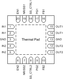
5 Pin Configuration and Functions
RTJ Package
4-mm × 4-mm 20-Pin WQFN
Top View

Pin Functions
| PIN | DESCRIPTION | ||
|---|---|---|---|
| NAME | NO. | I/O | |
| EN1 | 20 | I | Enable pin for each channel. These pins turn the regulator on and off. If VENx(1) ≥ VIH(ENx), the regulator is enabled. If VENx ≤ VIL(ENx), the regulator is disabled. The ENx pin must be connected to INx if the enable function is not used. |
| EN2 | 6 | ||
| FB1 | 16 | I | Feedback pin for each channel. These pins are the inputs to the control loop error amplifier and are used to set the output voltage of the device. |
| FB2 | 10 | ||
| GND | 3, 13 | — | Device GND. Connect both pins to the device thermal pad. |
| IN1 | 1, 2 | I | Input pin for LDO1. A 10 µF or greater input capacitor is required to assure robust operation. |
| IN2 | 4, 5 | Input pin for LDO2. A 10 µF or greater input capacitor is required to assure robust operation. | |
| NR/SS1 | 19 | — | Noise reduction pin for each channel. Connect these pins to an external capacitor to bypass the noise generated by the internal band-gap reference. The capacitor reduces the output RMS noise to very low levels and sets the output ramp rate to limit inrush current. |
| NR/SS2 | 7 | ||
| OUT1 | 14, 15 | O | Regulated output 1. A 10 µF or greater capacitor must be connected from this pin to GND to assure stability. |
| OUT2 | 11, 12 | Regulated output 2. A 10 µF or greater capacitor must be connected from this pin to GND to assure stability. | |
| PG1 | 17 | O | Open-drain power-good indicator pins for the LDO1 and LDO2 output voltages. A 10-kΩ to 100-kΩ external pullup resistor is required. These pins can be left floating or connected to GND if not used. |
| PG2 | 9 | ||
| SS_CTRL1 | 18 | I | Soft-start control pin for each channel. Connect these pins either to GND or INx to allow normal or fast charging of the NR/SSx capacitor. If a CNR/SSx capacitor is not used, SS_CTRLx must be connected to GND to avoid output overshoot. |
| SS_CTRL2 | 8 | ||
| Thermal pad | — | Connect the thermal pad to the printed circuit board (PCB) ground plane. | |
(1) Lowercase x indicates that the specification under consideration applies to both channel 1 and channel 2, one channel at a time.