ZHCSFW2 December 2016 TPS7A91
PRODUCTION DATA.
- 1 特性
- 2 应用
- 3 说明
- 4 修订历史记录
- 5 Pin Configuration and Functions
- 6 Specifications
-
7 Detailed Description
- 7.1 Overview
- 7.2 Functional Block Diagram
- 7.3 Feature Description
- 7.4 Device Functional Modes
- 8 Application and Implementation
- 9 Power Supply Recommendations
- 10Layout
- 11器件和文档支持
- 12机械、封装和可订购信息
8 Application and Implementation
NOTE
Information in the following applications sections is not part of the TI component specification, and TI does not warrant its accuracy or completeness. TI’s customers are responsible for determining suitability of components for their purposes. Customers should validate and test their design implementation to confirm system functionality.
8.1 Application Information
The TPS7A91 is a linear voltage regulator operating from 1.4 V to 6.5 V on the input and regulates voltages between 0.8 V to 5.0 V within 1% accuracy and a 1-A maximum output current. Efficiency is defined by the ratio of output voltage to input voltage because the TPS7A91 is a linear voltage regulator. To achieve high efficiency, the dropout voltage (VIN – VOUT) must be as small as possible, thus requiring a very low dropout LDO. Successfully implementing an LDO in an application depends on the application requirements. This section discusses key device features and how to best implement them to achieve a reliable design.
8.1.1 Adjustable Output
The output voltage of the TPS7A9101 can be adjusted from 0.8 V to 5.2 V by using a resistor divider network as shown in Figure 38.
 Figure 38. Adjustable Operation
R1 and R2 can be calculated for any output voltage range using Equation 3. This resistive network must provide a current greater than or equal to 5 μA for optimum noise performance.

If greater voltage accuracy is required, take into account the output voltage offset contribution resulting from the feedback pin current (IFB) and use 0.1%-tolerance resistors.
Table 2 lists the resistor combination required to achieve a few of the most common rails using commercially-available, 0.1%-tolerance resistors to maximize nominal voltage accuracy and also abiding to the formula given in Equation 3.
Table 2. Recommended Feedback-Resistor Values
| VOUT(TARGET)
(V) |
FEEDBACK RESISTOR VALUES (1) | CALCULATED OUTPUT VOLTAGE (V) | |
|---|---|---|---|
| R1 (kΩ) | R2 (kΩ) | ||
| 0.8 | Short | Open | 0.800 |
| 1.00 | 2.55 | 10.2 | 1.000 |
| 1.20 | 5.9 | 11.8 | 1.200 |
| 1.50 | 9.31 | 10.7 | 1.496 |
| 1.80 | 1.87 | 1.5 | 1.797 |
| 1.90 | 15.8 | 11.5 | 1.899 |
| 2.50 | 2.43 | 1.15 | 2.490 |
| 3.00 | 3.16 | 1.15 | 2.998 |
| 3.30 | 3.57 | 1.15 | 3.283 |
| 5.00 | 10.5 | 2 | 5.00 |
8.1.2 Start-Up
8.1.2.1 Enable (EN) and Undervoltage Lockout (UVLO)
The TPS7A91 only turns on when EN and UVLO are above the respective voltage thresholds. The TPS7A91 has an independent UVLO circuit that monitors the input voltage to allow a controlled and consistent turn on and off. The UVLO has approximately 290 mV of hysteresis to prevent the device from turning off if the input drops during turn on. The EN signal allows independent logic-level turn-on and shutdown of the LDO when the input voltage is present. Connecting EN directly to IN is recommended if independent turn-on is not needed.
The TPS7A91 has an internal pulldown MOSFET that connects a discharge resistor from VOUT to ground when the device is disabled to actively discharge the output voltage.
8.1.2.2 Noise-Reduction and Soft-Start Capacitor (CNR/SS)
The CNR/SS capacitor serves a dual purpose of both reducing output noise and setting the soft-start ramp during turn-on.
8.1.2.2.1 Noise Reduction
For low-noise applications, the CNR/SS capacitor forms an RC filter for filtering output noise that is otherwise amplified by the control loop. For low-noise applications, a CNR/SS of between 10 nF to 10 µF is recommended. Larger values for CNR/SS can be used; however, above 1 µF there is little benefit in lowering the output voltage noise for frequencies above 10 Hz.
8.1.2.2.2 Soft-Start and Inrush Current
Soft-start refers to the gradual ramp-up characteristic of the output voltage after the EN and UVLO thresholds are exceeded. Reducing how quickly the output voltage increases during startup also reduces the amount of current needed to charge the output capacitor, referred to as inrush current. Inrush current is defined as the current going into the LDO during start-up. Inrush current consists of the load current, the current used to charge the output capacitor, and the ground pin current (that contributes very little to inrush current). This current is difficult to measure because the input capacitor must be removed, which is not recommended. However, the inrush current can be estimated by Equation 4:

where
- VOUT(t) is the instantaneous output voltage of the turn-on ramp
- dVOUT(t)/dt is the slope of the VOUT ramp and
- RLOAD is the resistive load impedance
The TPS7A91 features a monotonic, voltage-controlled soft-start that is set by the user with an external capacitor (CNR/SS). This soft-start helps reduce inrush current, minimizing load transients to the input power bus that can cause potential start-up initialization problems when powering FPGAs, digital signal processors (DSPs), or other high current loads.
To achieve a monotonic start-up, the TPS7A91 error amplifier tracks the voltage ramp of the external soft-start capacitor until the voltage exceeds approximately 97% of the internal reference. The final 3% of VNR/SS is charged through the noise-reduction resistor (RNR), creating an RC delay. RNR is approximately 280 kΩ and applications that require the highest accuracy when using a large value CNR/SS must take this RC delay into account.
The soft-start ramp time depends on the soft-start charging current (INR/SS), the soft-start capacitance (CNR/SS), and the internal reference (VREF). The approximate soft-start ramp time (tSS) can be calculated with Equation 5:
Note that the value for INR/SS is determined by the state of the SS_CTRL pin. When the SS_CTRL pin is connected to GND, the typical value for the INR/SS current is 6.2 µA. Connecting the SS_CTRL pin to IN increases the typical soft-start charging current to 100 µA. The larger charging current for INR/SS is useful if shorter start-up times are needed (such as when using a large noise-reduction capacitor).
8.1.3 Capacitor Recommendation
The TPS7A91 is designed to be stable using low equivalent series resistance (ESR) ceramic capacitors at the input, output, and noise-reduction pin. Multilayer ceramic capacitors have become the industry standard for these types of applications and are recommended, but must be used with good understanding of their limitations. Ceramic capacitors that employ X7R-, X5R-, and COG-rated dielectric materials provide relatively good capacitive stability across temperature, whereas the use of Y5V-rated capacitors is discouraged precisely because the capacitance varies so widely. In all cases, ceramic capacitors vary a great deal with operating voltage and temperature and the design engineer must be aware of these characteristics. As a rule of thumb, ceramic capacitors are recommended to be derated by 50%. The input and output capacitors recommended herein account for a capacitance derating of 50%.
8.1.3.1 Input and Output Capacitor Requirements (CIN and COUT)
The TPS7A91 is designed and characterized for operation with ceramic capacitors of 10 µF or greater at the input and output. Locate the input and output capacitors as near as practical to the input and output pins to minimize the trace inductance from the capacitor to the device.
Attention must be given to the input capacitance to minimize transient input droop during startup and load current steps. Note that simply using very large ceramic input capacitances can cause unwanted ringing at the output if the input capacitor (in combination with the wire-lead inductance) creates a high-Q peaking effect during transients, which is why short, well-designed interconnect traces to the upstream supply are needed to minimize ringing. Damping of unwanted ringing can be accomplished by using a tantalum capacitor, with a few hundred milliohms of ESR, in parallel with the ceramic input capacitor. The UVLO circuit responds quickly to glitches on VIN and disables the output of the device if this rail starts to collapse too quickly. Use an input capacitor that is large enough to slow input transients to less then two volts per microsecond.
8.1.3.1.1 Load-Step Transient Response
The load-step transient response is the output voltage response by the LDO to a step change in load current. The depth of charge depletion immediately after the load step is directly proportional to the amount of output capacitance. However, although larger output capacitances decrease any voltage dip or peak occurring during a load step, the control-loop bandwidth is also decreased, thereby slowing the response time.
The LDO cannot sink charge, therefore when the output load is removed or greatly reduced, the control loop must turn off the pass-FET and wait for any excess charge to deplete.
8.1.3.2 Feed-Forward Capacitor (CFF)
Although a feed-forward capacitor (CFF), from the FB pin to the OUT pin is not required to achieve stability, a 10-nF, feed-forward capacitor improves the noise and PSRR performance. A higher capacitance CFF can be used; however, the startup time is longer and the power-good signal can incorrectly indicate that the output voltage has settled. For a detailed description, see the Pros and Cons of Using a Feedforward Capacitor with a Low-Dropout Regulator application report (SBVA042).
8.1.4 Power Dissipation (PD)
Circuit reliability demands that proper consideration be given to device power dissipation, location of the circuit on the printed circuit board (PCB), and correct sizing of the thermal plane. The PCB area around the regulator must be as free as possible of other heat-generating devices that cause added thermal stresses.
To first-order approximation, power dissipation in the regulator depends on the input-to-output voltage difference and load conditions. PD can be calculated using Equation 6:
An important note is that power dissipation can be minimized, and thus greater efficiency achieved, by proper selection of the system voltage rails. For the lowest power dissipation use the minimum input voltage necessary for proper output regulation.
The primary heat conduction path for the DSK package is through the thermal pad to the PCB. Solder the thermal pad to a copper pad area under the device. This pad area should contain an array of plated vias that conduct heat to additional copper planes for increased heat dissipation.
The maximum power dissipation determines the maximum allowable ambient temperature (TA) for the device. Power dissipation and junction temperature are most often related by the junction-to-ambient thermal resistance (θJA) of the combined PCB and device package and the temperature of the ambient air (TA), according to Equation 7.

Unfortunately, the thermal resistance (θJA) is highly dependent on the heat-spreading capability built into the particular PCB design, and therefore varies according to the total copper area, copper weight, and location of the planes. The θJA recorded in the Thermal Information table is determined by the JEDEC standard, PCB, and copper-spreading area and is only used as a relative measure of package thermal performance.
8.1.5 Estimating Junction Temperature
The JEDEC standard now recommends the use of psi (Ψ) thermal metrics to estimate the junction temperatures of the LDO when in-circuit on a typical PCB board application. These metrics are not strictly speaking thermal resistances, but rather offer practical and relative means of estimating junction temperatures. These psi metrics are determined to be significantly independent of the copper-spreading area. The key thermal metrics (ΨJT and ΨJB) are given in the Thermal Information table and are used in accordance with Equation 8.

where
- PD is the power dissipated as explained in Equation 6
- TT is the temperature at the center-top of the device package and
- TB is the PCB surface temperature measured 1 mm from the device package and centered on the package edge
For a more detailed discussion on thermal metrics and how to use them, see the Semiconductor and IC Package Thermal Metrics application report (SPRA953).
8.2 Typical Application
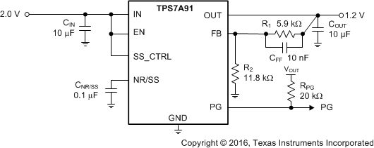
This section discusses the implementation of the TPS7A91 to regulate from a 2-V input voltage to a 1.2-V output voltages for noise-sensitive loads. The schematic for this application circuit is provided in Figure 39.
 Figure 39. Application Example
8.2.1 Design Requirements
For the design example shown in Figure 39, use the parameters listed in Table 3 as the input parameters.
Table 3. Design Parameters
| PARAMETER | APPLICATION REQUIREMENTS | DESIGN RESULTS |
|---|---|---|
| Input voltages (VIN) | 2 V, ±3%, provided by the dc-dc converter switching at 750 kHz | 1.4 V to 6.5 V |
| Maximum ambient operating temperature | 55°C | 101°C junction temperature |
| Output voltages (VOUT) | 1.2 V, ±1% | 1.2 V, ±1% |
| Output currents (IOUT) | 1.0 A (max), 10 mA (min) | 1.0 A (max), 5 mA (min) |
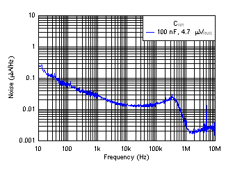
| RMS noise | < 5 µVRMS, bandwidth = 10 Hz to 100 kHz | 4.7 µVRMS, bandwidth = 10 Hz to 100 kHz |
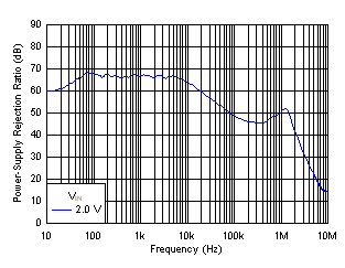
| PSRR at 750 kHz | > 40 dB | 49 dB |
| Startup time | < 2 ms | 800 µs (typ) 1.48 µs (max) |
8.2.2 Detailed Design Procedure
The output voltage can be set to 1.2 V by selecting the correct values for R1 and R2; see Equation 3.
Input and output capacitors are selected in accordance with the Capacitor Recommendation section. Ceramic capacitances of 10 µF for both input and output are selected to help balance the charge needed during startup when charging the output capacitor, thus reducing the input voltage drop.
To satisfy the required startup time (tSS) and still maintain low-noise performance, a 0.1-µF CNR/SS is selected for with SS_CTRL connected to VIN. This value is calculated with Equation 9. Using the INR/SS(MAX) and the smallest CNR/SS capacitance resulting from manufacturing variance (often ±20%) provides the fastest startup time, whereas using the INR/SS(MIN) and the largest CNR/SS capacitance resulting from manufacturing variance provides the slowest startup time.
With a 1.0-A maximum load, the internal power dissipation is 800 mW, corresponding to a 46°C junction temperature rise. With an 55°C maximum ambient temperature, the junction temperature is at 101°C. To minimize noise, a feed-forward capacitance (CFF) of 10 nF is selected.
See the Layout section for an example of how to layout the TPS7A91 to achieve best PSRR and noise.
8.2.3 Application Curves

