ZHCSOO0C september 2021 – june 2023 TPS7A94
PRODUCTION DATA
- 1
- 1 特性
- 2 应用
- 3 说明
- 4 Revision History
- 5 Pin Configuration and Functions
- 6 Specifications
-
7 Detailed Description
- 7.1 Overview
- 7.2 Functional Block Diagram
- 7.3
Feature Description
- 7.3.1 Output Voltage Setting and Regulation
- 7.3.2 Ultra-Low Noise and Ultra-High Power-Supply Rejection Ratio (PSRR)
- 7.3.3 Programmable Current Limit and Power-Good Threshold
- 7.3.4 Programmable Soft Start (NR/SS Pin)
- 7.3.5 Precision Enable and UVLO
- 7.3.6 Active Discharge
- 7.3.7 Thermal Shutdown Protection (TSD)
- 7.4 Device Functional Modes
-
8 Application and Implementation
- 8.1
Application Information
- 8.1.1 Output Voltage Restart (Overshoot Prevention Circuit)
- 8.1.2 Precision Enable (External UVLO)
- 8.1.3 Undervoltage Lockout (UVLO) Operation
- 8.1.4 Dropout Voltage (VDO)
- 8.1.5 Power-Good Feedback (FB_PG Pin) and Power-Good Threshold (PG Pin)
- 8.1.6 Adjusting the Factory-Programmed Current Limit
- 8.1.7 Programmable Soft-Start and Noise-Reduction (NR/SS Pin)
- 8.1.8 Inrush Current
- 8.1.9 Optimizing Noise and PSRR
- 8.1.10 Adjustable Operation
- 8.1.11 Paralleling for Higher Output Current and Lower Noise
- 8.1.12 Recommended Capacitor Types
- 8.1.13 Load Transient Response
- 8.1.14 Power Dissipation (PD)
- 8.1.15 Estimating Junction Temperature
- 8.1.16 TPS7A94EVM-046 Thermal Analysis
- 8.2 Typical Application
- 8.3 Power Supply Recommendations
- 8.4 Layout
- 8.1
Application Information
- 9 Device and Documentation Support
- 10Mechanical, Packaging, and Orderable Information
8.1.9 Optimizing Noise and PSRR
Noise can be generally defined as any unwanted signal combining with the desired signal (such as the regulated LDO output). Noise can easily be noticed in audio as a hissing or popping sound. Noise produced from an external circuit or the 50- to 60-hertz power-line noise (spikes), along with the harmonics, is an excellent representative of extrinsic noise. Intrinsic noise is produced by components within the device circuitry, such as resistors and transistors. The two dominating sources of intrinsic noise are the error amplifier and the internal reference voltage (VNR/SS). Extrinsic noise, including the switching mode power-supply ac ripple voltage, coupled onto the input supply of the LDO is attenuated by the LDO power-supply rejection ratio, or PSRR. PSRR is a measurement of the noise attenuation from the input to the output of the LDO.
Optimize the intrinsic noise and PSRR by carefully selecting:
- CNR/SS for the low-frequency range up to the device bandwidth
- COUT for the high-frequency range close to and higher than the device bandwidth
- Operating headroom, VIN – VOUT (VDO), mainly for the low-frequency range up to the device bandwidth, but also for higher frequencies to a lesser effect
These behaviors are described in the Typical Characteristics curves.
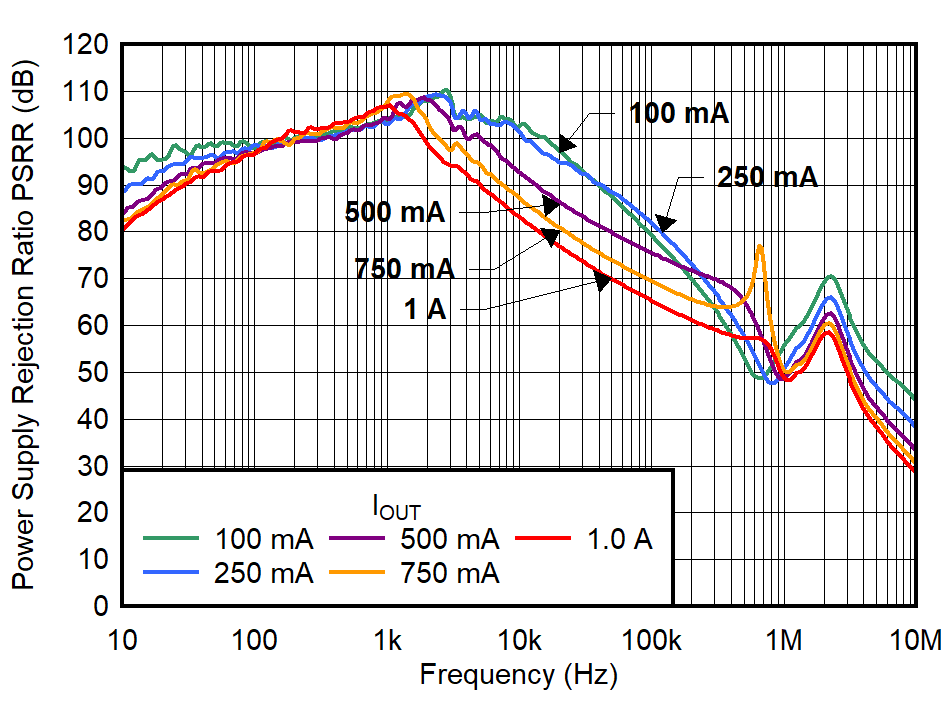
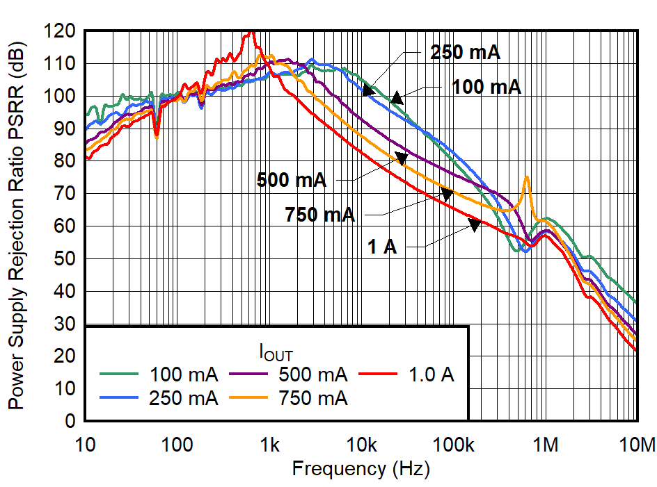
Figure 8-14 and Figure 8-15 show the measured 10-Hz to 100-kHz RMS noise for a 3.3-V device output voltage with a 0.5-V headroom for different CNR/SS and COUT capacitors and a 1-A load current. Table 8-3 lists the typical output noise for these capacitors.
 Figure 8-14 PSRR vs Frequency and
IOUT for VOUT = 3.3 V, COUT = 10
μF
 Figure 8-15 PSRR vs Frequency and
IOUT for VOUT = 3.3 V, COUT = 4.7 μF ||
4.7 μF|| 1.0 μF
Figure 8-15 PSRR vs Frequency and
IOUT for VOUT = 3.3 V, COUT = 4.7 μF ||
4.7 μF|| 1.0 μF| Vn (μVRMS), 10-Hz to 100-kHz BW | CNR/SS (µF) | COUT (µF) | START-UP TIME (ms) |
|---|---|---|---|
| 0.98 | 1 | 10 | 3.73 |
| 0.62 | 2.2 | 10 | 6.21 |
| 0.46 | 4.7 | 10 | 13.97 |
| 0.42 | 10 | 10 | 28.21 |
PSRR can be viewed as being simply the ratio of the output capacitor impedance by the LDO output impedance. At low frequency, the output impedance is very low whereas the output impedance of the capacitor is high, resulting in high PSRR. As the frequency increases, the output capacitor impedance reduces and reaches a minima set by the ESR.
As shown in Figure 8-14 and Figure 8-15, and in order to achieve high PSRR at high frequencies, ensure that the output capacitor ESR and ESL are minimal. These figures compare the use of a single 10-μF output capacitor with a 4.7-μF || 4.7-μF || 1.0-μF implementation. Notice that below 200 kHz, there is no impact on performance but above 200 kHz, the PSRR improves by 5 dB to 7 dB.
Minimizing the ESR, ESL generated resonance point in the output capacitance allows for a smoother transition between the LDO active PSRR component to the passive PSRR of the capacitors.