ZHCSOO0C september 2021 – june 2023 TPS7A94
PRODUCTION DATA
- 1
- 1 特性
- 2 应用
- 3 说明
- 4 Revision History
- 5 Pin Configuration and Functions
- 6 Specifications
-
7 Detailed Description
- 7.1 Overview
- 7.2 Functional Block Diagram
- 7.3
Feature Description
- 7.3.1 Output Voltage Setting and Regulation
- 7.3.2 Ultra-Low Noise and Ultra-High Power-Supply Rejection Ratio (PSRR)
- 7.3.3 Programmable Current Limit and Power-Good Threshold
- 7.3.4 Programmable Soft Start (NR/SS Pin)
- 7.3.5 Precision Enable and UVLO
- 7.3.6 Active Discharge
- 7.3.7 Thermal Shutdown Protection (TSD)
- 7.4 Device Functional Modes
-
8 Application and Implementation
- 8.1
Application Information
- 8.1.1 Output Voltage Restart (Overshoot Prevention Circuit)
- 8.1.2 Precision Enable (External UVLO)
- 8.1.3 Undervoltage Lockout (UVLO) Operation
- 8.1.4 Dropout Voltage (VDO)
- 8.1.5 Power-Good Feedback (FB_PG Pin) and Power-Good Threshold (PG Pin)
- 8.1.6 Adjusting the Factory-Programmed Current Limit
- 8.1.7 Programmable Soft-Start and Noise-Reduction (NR/SS Pin)
- 8.1.8 Inrush Current
- 8.1.9 Optimizing Noise and PSRR
- 8.1.10 Adjustable Operation
- 8.1.11 Paralleling for Higher Output Current and Lower Noise
- 8.1.12 Recommended Capacitor Types
- 8.1.13 Load Transient Response
- 8.1.14 Power Dissipation (PD)
- 8.1.15 Estimating Junction Temperature
- 8.1.16 TPS7A94EVM-046 Thermal Analysis
- 8.2 Typical Application
- 8.3 Power Supply Recommendations
- 8.4 Layout
- 8.1
Application Information
- 9 Device and Documentation Support
- 10Mechanical, Packaging, and Orderable Information
8.1.16 TPS7A94EVM-046 Thermal Analysis
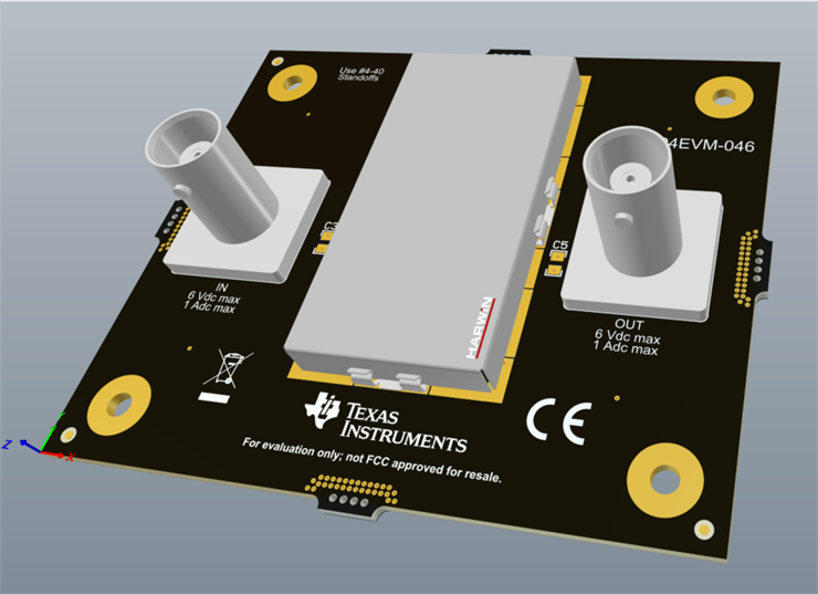
The TPS7A94EVM-046 EVM was used to develop the TPS7A9401DRC thermal model. The DRC package is a 3-mm × 3-mm, 10-pin VQFN with 25-µm plating on each via. The EVM is a 2.85-inch × 3.35-inch (72.39 mm × 85.09 mm) PCB comprised of four layers. Table 8-5 lists the layer stackup for the EVM. Figure 8-19 to Figure 8-23 illustrate the various layer details for the EVM.
| LAYER | NAME | MATERIAL | THICKNESS (mil) |
|---|---|---|---|
| 1 | Top overlay | — | — |
| 2 | Top solder | Solder resist | 0.4 |
| 3 | Top layer | Copper | 2.8 |
| 4 | Dielectric 1 | FR-4 high Tg | 10 |
| 5 | Mid layer 1 | Copper | 2.8 |
| 6 | Dielectric 2 | FR-4 high Tg | 30 |
| 7 | Mid layer 2 | Copper | 2.8 |
| 8 | Dielectric 3 | FR-4 high Tg | 10 |
| 9 | Bottom layer | Copper | 2.8 |
| 10 | Bottom solder | Solder resist | 0.4 |
 Figure 8-19 Top
Composite View
 Figure 8-21 Mid
Layer 1 Routing
 Figure 8-23 Bottom Layer Routing
 Figure 8-20 Top
Layer Routing
 Figure 8-22 Mid
Layer 2 Routing
Figure 8-22 Mid
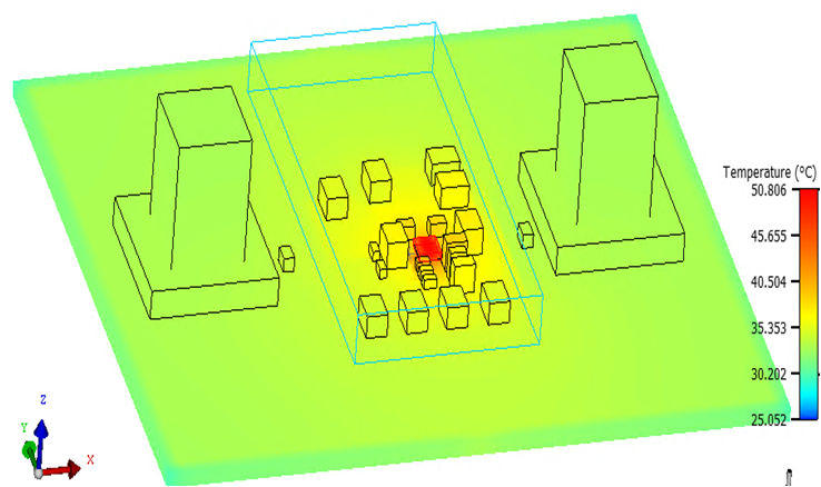
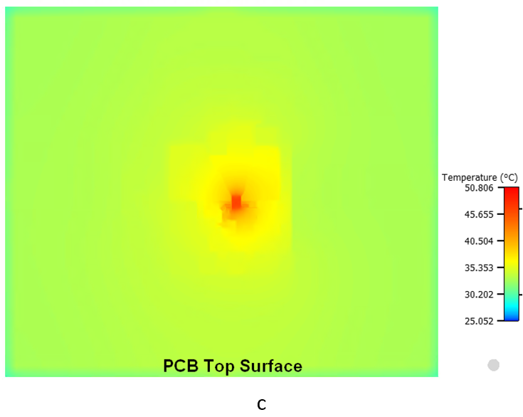
Layer 2 RoutingFigure 8-24 to Figure 8-26 show the thermal gradient on the PCB and device that results when a 1-W power dissipation is used through the pass transistor with a 25°C ambient temperature. Table 8-6 shows thermal simulation data for the TPS7A94EVM-046.
| DUT | RθJA (°C/W) | ⍦JB (°C/W) | ⍦JT (°C/W) |
|---|---|---|---|
| TPS7A94EVM-046 | 25.6 | 11.5 | 0.3 |

 Figure 8-26 TPS7A94EVM-046 Device
Thermal Gradient
 Figure 8-25 TPS7A94EVM-046 PCB Thermal
Gradient