ZHCSOO0C september 2021 – june 2023 TPS7A94
PRODUCTION DATA
- 1
- 1 特性
- 2 应用
- 3 说明
- 4 Revision History
- 5 Pin Configuration and Functions
- 6 Specifications
-
7 Detailed Description
- 7.1 Overview
- 7.2 Functional Block Diagram
- 7.3
Feature Description
- 7.3.1 Output Voltage Setting and Regulation
- 7.3.2 Ultra-Low Noise and Ultra-High Power-Supply Rejection Ratio (PSRR)
- 7.3.3 Programmable Current Limit and Power-Good Threshold
- 7.3.4 Programmable Soft Start (NR/SS Pin)
- 7.3.5 Precision Enable and UVLO
- 7.3.6 Active Discharge
- 7.3.7 Thermal Shutdown Protection (TSD)
- 7.4 Device Functional Modes
-
8 Application and Implementation
- 8.1
Application Information
- 8.1.1 Output Voltage Restart (Overshoot Prevention Circuit)
- 8.1.2 Precision Enable (External UVLO)
- 8.1.3 Undervoltage Lockout (UVLO) Operation
- 8.1.4 Dropout Voltage (VDO)
- 8.1.5 Power-Good Feedback (FB_PG Pin) and Power-Good Threshold (PG Pin)
- 8.1.6 Adjusting the Factory-Programmed Current Limit
- 8.1.7 Programmable Soft-Start and Noise-Reduction (NR/SS Pin)
- 8.1.8 Inrush Current
- 8.1.9 Optimizing Noise and PSRR
- 8.1.10 Adjustable Operation
- 8.1.11 Paralleling for Higher Output Current and Lower Noise
- 8.1.12 Recommended Capacitor Types
- 8.1.13 Load Transient Response
- 8.1.14 Power Dissipation (PD)
- 8.1.15 Estimating Junction Temperature
- 8.1.16 TPS7A94EVM-046 Thermal Analysis
- 8.2 Typical Application
- 8.3 Power Supply Recommendations
- 8.4 Layout
- 8.1
Application Information
- 9 Device and Documentation Support
- 10Mechanical, Packaging, and Orderable Information
8.1.6 Adjusting the Factory-Programmed Current Limit
The current limit is a brick-wall scheme and
the factory-programmed current limit value can be programmed to a set of discrete value
(100%, 80%, or 60% of the default value), as specified in the Electrical CharacteristicsElectrical CharacteristicsElectrical CharacteristicsElectrical CharacteristicsElectrical CharacteristicsElectrical CharacteristicsElectrical Characteristics table. This adjustment can be done by changing the input impedance of the
FB_PG pin represented by the parallel resistance of RFB_PG(TOP) ||
RFB_PG(BOTTOM). The FB_PG pin has dual functionality: adjusting the
ICL value and setting the power-good (PG) assert threshold.
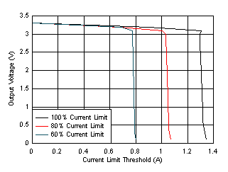
 Figure 8-9 Programmable Current Limit
Behavior (Typical) for a 3.3-VOUT(nom)
Prior to start up, the input impedance of the FB_PG pin is sampled and the ICL value is adjusted based on the input impedance.
Note:
The current limit programmability is dependent on the output voltage. For voltages below 0.4 V, the current limit cannot be programmed. For voltages between 0.4 V and 1.2 V, the current limit cannot be adjusted and is always set to 100%. Table 8-1 describes this behavior.
Table 8-1 Programmable Current Limit vs
Output Voltage
| NOMINAL OUTPUT VOLTAGE (V) | RFB_PG(BOTTOM) (kΩ) | RFB_PG(TOP) (kΩ) | ICL SETTING (%) |
|---|---|---|---|
| VOUT(nom) ≥ 1.2 V |
RFB_PG(BOTTOM) = 0.2 V
/ 16 μA
|
RFB_PG(TOP) = RFB_PG(BOTTOM) × (
VOUT(nom) / 0.2 V × K – 1) with
K = PG threshold (%VOUT) |
100 |
|
RFB_PG(BOTTOM) = 0.2 V
/ 4 μA
|
80 | ||
|
RFB_PG(BOTTOM) = 0.2 V
/ 2 μA
|
60 | ||
| 0.4 V ≤ VOUT(nom) < 1.2 V |
RFB_PG(BOTTOM) = 0.2 V
/ 6 μA
|
100 | |
| VOUT(nom) < 0.4 V | N/A | N/A | N/A |
Table 8-2 provides values for various output voltages using 1% resistors.
Table 8-2 Programmable Current Limit
Voltage-Divider Current Settings
| NOMINAL OUTPUT VOLTAGE (V) | RFB_PG(BOTTOM) (kΩ) | RFB_PG(TOP) (kΩ) | ICL SETTING (%) | PG THRESHOLD (%) |
|---|---|---|---|---|
| VOUT(nom) = 1.2 V | 12.4 | 51.1 | 100 | 85 |
| 49.9 | 205 | 80 | 85 | |
| 100 | 412 | 60 | 85 | |
| VOUT(nom) = 3.3 V | 12.4 | 187 | 100 | 95 |
| 49.9 | 732 | 80 | 95 | |
| 100 | 1470 | 60 | 95 | |
| VOUT(nom) = 5.1 V | 12.4 | 287 | 100 | 95 |
| 49.9 | 1150 | 80 | 95 | |
| 100 | 2320 | 60 | 95 |
Figure 8-9 shows the different ICL settings for a nominal 3.3-V output voltage.
 Figure 8-9 Programmable Current Limit
Behavior (Typical) for a 3.3-VOUT(nom)