ZHCSOO0C september 2021 – june 2023 TPS7A94
PRODUCTION DATA
- 1
- 1 特性
- 2 应用
- 3 说明
- 4 Revision History
- 5 Pin Configuration and Functions
- 6 Specifications
-
7 Detailed Description
- 7.1 Overview
- 7.2 Functional Block Diagram
- 7.3
Feature Description
- 7.3.1 Output Voltage Setting and Regulation
- 7.3.2 Ultra-Low Noise and Ultra-High Power-Supply Rejection Ratio (PSRR)
- 7.3.3 Programmable Current Limit and Power-Good Threshold
- 7.3.4 Programmable Soft Start (NR/SS Pin)
- 7.3.5 Precision Enable and UVLO
- 7.3.6 Active Discharge
- 7.3.7 Thermal Shutdown Protection (TSD)
- 7.4 Device Functional Modes
-
8 Application and Implementation
- 8.1
Application Information
- 8.1.1 Output Voltage Restart (Overshoot Prevention Circuit)
- 8.1.2 Precision Enable (External UVLO)
- 8.1.3 Undervoltage Lockout (UVLO) Operation
- 8.1.4 Dropout Voltage (VDO)
- 8.1.5 Power-Good Feedback (FB_PG Pin) and Power-Good Threshold (PG Pin)
- 8.1.6 Adjusting the Factory-Programmed Current Limit
- 8.1.7 Programmable Soft-Start and Noise-Reduction (NR/SS Pin)
- 8.1.8 Inrush Current
- 8.1.9 Optimizing Noise and PSRR
- 8.1.10 Adjustable Operation
- 8.1.11 Paralleling for Higher Output Current and Lower Noise
- 8.1.12 Recommended Capacitor Types
- 8.1.13 Load Transient Response
- 8.1.14 Power Dissipation (PD)
- 8.1.15 Estimating Junction Temperature
- 8.1.16 TPS7A94EVM-046 Thermal Analysis
- 8.2 Typical Application
- 8.3 Power Supply Recommendations
- 8.4 Layout
- 8.1
Application Information
- 9 Device and Documentation Support
- 10Mechanical, Packaging, and Orderable Information
8.1.2 Precision Enable (External UVLO)
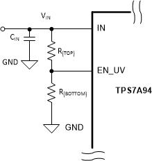
The precision enable circuit is used to turn the device on and off. This circuit can be used to set an external undervoltage lockout (UVLO) voltage (see Figure 8-6) to turn on and off the device using a resistor divider between IN, EN_UV, and GND.
If VEN_UV ≥ VIH(EN_UV), the regulator is enabled. If VEN_UV ≤ VIL(EN_UV), the regulator is disabled. The EN_UV pin does not incorporate an internal pulldown resistor to GND and must not be left floating. Use the precision enable circuit for this pin to set an external undervoltage lockout (UVLO) input supply voltage to turn on and off the device using a resistor divider between IN, EN_UV, and GND.
 Figure 8-6 Precision EN Used as External
UVLO
Figure 8-6 Precision EN Used as External
UVLOThis external UVLO configuration prevents the LDO from turning on when the input supply voltage is insufficient and places the device in dropout operation.
Using the EN_UV pin as an externally set UVLO allows simple sequencing of cascaded power supplies. An additional benefit is that the EN_UV pin is never left floating. The EN_UV pin does not have an internal pulldown resistor. In addition to the resistor divider, a zener diode can be needed between the EN_UV pin and ground to comply with the absolute maximum ratings on this pin.
When VIN exceeds the targeted VON voltage and the R(BOTTOM) resistor is set, Equation 1 and Equation 2 provide the R(TOP) resistor value and the VOFF voltage at which the input voltage must drop below to disable the LDO.
where:
- VOFF is the input voltage where the regulator shuts off
- VON is the voltage where the regulator turns on
Consider the EN_UV current pin when selecting the R(TOP) and R(BOTTOM) values.