ZHCSBU7B October   2013  – July 2015 TPS7B4250-Q1

PRODUCTION DATA.  

  1. 特性
  2. 应用
  3. 说明
  4. 修订历史记录
  5. Pin Configuration and Functions
  6. Specifications
    1. 6.1 Absolute Maximum Ratings
    2. 6.2 ESD Ratings
    3. 6.3 Recommended Operating Conditions
    4. 6.4 Thermal Information
    5. 6.5 Electrical Characteristics
    6. 6.6 Typical Characteristics
  7. Detailed Description
    1. 7.1 Overview
    2. 7.2 Functional Block Diagram
    3. 7.3 Feature Description
      1. 7.3.1 Regulated Output (VOUT)
      2. 7.3.2 Undervoltage Shutdown
      3. 7.3.3 Thermal Protection
      4. 7.3.4 VOUT Short to Battery
      5. 7.3.5 Tracking Regulator with ENABLE Circuit
    4. 7.4 Device Functional Modes
      1. 7.4.1 Operation With VI < 4 V
      2. 7.4.2 Operation With ADJ/EN Control
  8. Application and Implementation
    1. 8.1 Application Information
    2. 8.2 Typical Application
      1. 8.2.1 Design Requirements
      2. 8.2.2 Detailed Design Procedure
        1. 8.2.2.1 External Capacitors
      3. 8.2.3 Application Curves
  9. Power Supply Recommendations
  10. 10Layout
    1. 10.1 Layout Guidelines
      1. 10.1.1 Package Mounting
      2. 10.1.2 Board Layout Recommendations to Improve PSRR and Noise Performance
    2. 10.2 Layout Example
    3. 10.3 Power Dissipation and Thermal Considerations
  11. 11器件和文档支持
    1. 11.1 文档支持
      1. 11.1.1 相关文档 
    2. 11.2 社区资源
    3. 11.3 商标
    4. 11.4 静电放电警告
    5. 11.5 Glossary
  12. 12机械、封装和可订购信息

封装选项

机械数据 (封装 | 引脚)
散热焊盘机械数据 (封装 | 引脚)
订购信息

5 Pin Configuration and Functions

DBV Package
5-Pin SOT-23
Top View
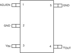
TPS7B4250-Q1 po_slvsca0.gif

Pin Functions

PIN TYPE DESCRIPTION
NAME NO.
ADJ/EN 1 I This pin connects to the reference voltage. A low signal disables the IC and a high signal enables the IC. Connected the voltage reference directly or with a voltage divider for lower output voltages. To compensate for line influences, TI recommends to place a capacitor close to the IC pins.
GND 2 G Internally connected to pin 5
5 Internally connected to pin 2
VIN 3 I This pin is the IC supply. To compensate for line influences, TI recommends to place a capacitor close to the IC pins.
VOUT 4 O VOUT is an external capacitor that is required between VOUT and GND with respect to the capacitance and ESR requirements given in the Recommended Operating Conditions.