ZHCSBU7B October 2013 – July 2015 TPS7B4250-Q1
PRODUCTION DATA.
7 Detailed Description
7.1 Overview
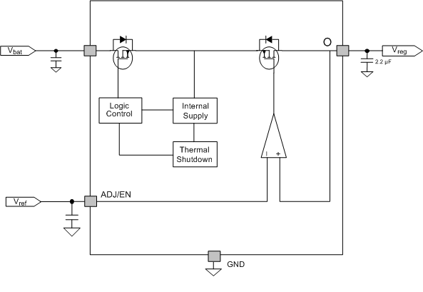
The TPS7B4250-Q1 device is a monolithic integrated low-dropout voltage tracker with ultra-low tracking tolerance. Several types of protection circuits are also integrated in the device such as output current limitation, reverse polarity protection, and thermal shutdown in case of over temperature.
7.3 Feature Description
7.3.1 Regulated Output (VOUT)
VOUT is the regulated output based on the reference voltage. The output has current limitation. During initial power up, the regulator has an incorporated soft start to control the initial current through the pass element.
7.3.2 Undervoltage Shutdown
The device has an internally-fixed undervoltage shutdown threshold. Undervoltage shutdown activates when the input voltage on VIN drops below UVLO. This activation ensures the regulator is not latched into an unknown state during low input supply voltage. If the input voltage has a negative transient that drops below the UVLO threshold and recovers, the regulator shuts down and powers up similar to a standard power-up sequence when the input voltage is above the required levels.
7.3.3 Thermal Protection
Thermal protection disables the output when the junction temperature rises to approximately 175°C which allows the device to cool. When the junction temperature cools to approximately 150°C, the output circuitry enables. Based on power dissipation, thermal resistance, and ambient temperature, the thermal protection circuit may cycle on and off. This cycling limits the dissipation of the regulator and protects it from damage as a result of overheating.
The internal protection circuitry of the TPS7B4250-Q1 device has been designed to protect against overload conditions. The circuitry was not intended to replace proper heat-sinking. Continuously running the TPS7B4250-Q1 device into thermal shutdown degrades device reliability.
7.3.4 VOUT Short to Battery
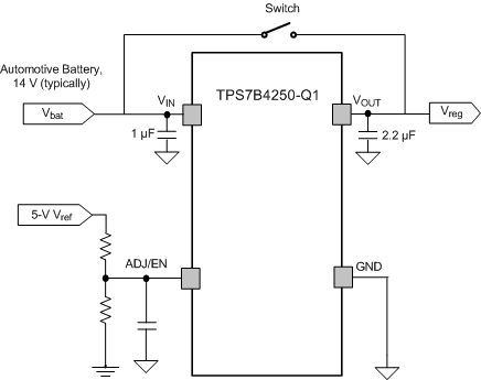
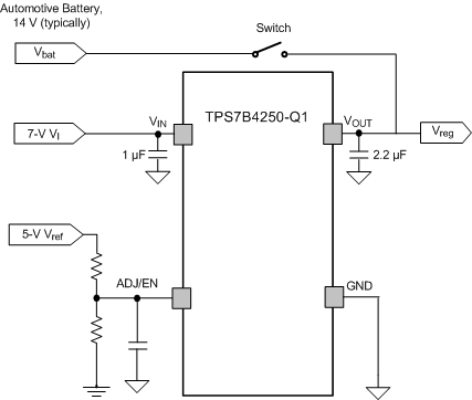
The TPS7B4250-Q1 device survives a short to battery when the output is shorted to the battery as shown in Figure 13. No damage occurs to the device. A short to the battery can also occur when the device is powered by an isolated supply at a lower voltage as shown in Figure 14. In this case the TPS7B4250-Q1 supply input voltage is set at 7 V when a short to battery (14 V typical) occurs on VOUT which typically runs at 5 V. The continuous reverse current flows out through VIN is less than 5 µA.
 Figure 13. Output-Voltage Short to Battery
 Figure 14. Output Voltage Higher than Input
7.3.5 Tracking Regulator with ENABLE Circuit
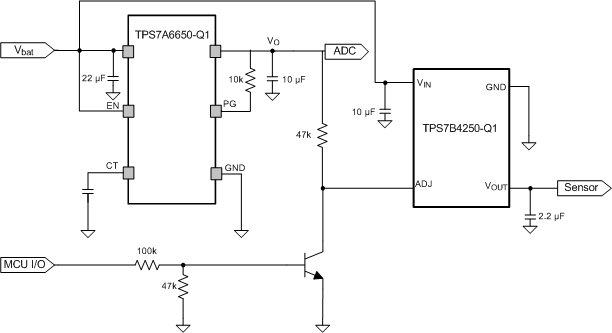
By pulling the reference voltage of the device below 0.8 V, the IC disables and enters a sleep state where the device draws 7.5 µA (typical) from the power supply. In a real application, the reference voltage is generally sourced from another LDO voltage rail. A case where the device must be disabled without a shutdown of the reference voltage can occur. In such case, the device can be configured as shown in Figure 15. The TPS7A6650-Q1 device is a 150-mA LDO with ultra-low quiescent current that is used as a reference voltage to the TPS7B4250-Q1 device and also as a power supply to the ADC. In a configuration as shown in Figure 15, the status of the device is controlled by an MCU I/O.
7.4 Device Functional Modes
7.4.1 Operation With VI < 4 V
The device operates with input voltages above 4 V. The maximum UVLO voltage is 3 V and operates at input voltage above 4 V. The device can also operate at lower input voltages; no minimum UVLO voltage is specified. At input voltages below the actual UVLO voltage, the device does not operate.
7.4.2 Operation With ADJ/EN Control
The rising-edge threshold voltage of the ADJ/EN pin is 1.5 V (maximum). When the EN pin is held above that voltage and the input voltage is above the 4 V, the device becomes active. The enable falling edge is 0.8 V (minimum). When the EN pin is held below that voltage the device is disabled, the IC quiescent current is reduced in this state.

