ZHCSF00A April   2016  – May 2016 TPS7B4254-Q1

PRODUCTION DATA.  

  1. 特性
  2. 应用
  3. 说明
  4. 修订历史记录
  5. Pin Configuration and Functions
  6. Specifications
    1. 6.1 Absolute Maximum Ratings
    2. 6.2 ESD Ratings
    3. 6.3 Recommended Operating Conditions
    4. 6.4 Thermal Information
    5. 6.5 Electrical Characteristics
    6. 6.6 Typical Characteristics
  7. Detailed Description
    1. 7.1 Overview
    2. 7.2 Functional Block Diagram
    3. 7.3 Feature Description
      1. 7.3.1 Short-Circuit and Overcurrent Protection
      2. 7.3.2 Integrated Inductive Clamp Protection
      3. 7.3.3 OUT Short-to-Battery and Reverse-Polarity Protection
      4. 7.3.4 Undervoltage Shutdown
      5. 7.3.5 Thermal Protection
      6. 7.3.6 Regulated Output (OUT)
      7. 7.3.7 Adjustable Output Voltage (FB and ADJ)
        1. 7.3.7.1 OUT Voltage Equal to the Reference Voltage
        2. 7.3.7.2 OUT Voltage Higher Than Reference Voltage
        3. 7.3.7.3 Output Voltage Lower Than Reference Voltage
    4. 7.4 Device Functional Modes
      1. 7.4.1 Operation With VIN < 4 V
  8. Application and Implementation
    1. 8.1 Application Information
    2. 8.2 Typical Applications
      1. 8.2.1 Application With Output Voltage Equal to the Reference Voltage
        1. 8.2.1.1 Design Requirements
        2. 8.2.1.2 Detailed Design Procedure
          1. 8.2.1.2.1 Input Capacitor
          2. 8.2.1.2.2 Output Capacitor
        3. 8.2.1.3 Application Curve
      2. 8.2.2 High-Accuracy LDO
  9. Power Supply Recommendations
  10. 10Layout
    1. 10.1 Layout Guidelines
    2. 10.2 Layout Example
  11. 11器件和文档支持
    1. 11.1 社区资源
    2. 11.2 商标
    3. 11.3 静电放电警告
    4. 11.4 Glossary
  12. 12机械、封装和可订购信息

封装选项

机械数据 (封装 | 引脚)
散热焊盘机械数据 (封装 | 引脚)
订购信息

10 Layout

10.1 Layout Guidelines

For the layout of the TPS7B4254-Q1 device, place the input and output capacitors close to the devices as shown in the Functional Block Diagram. To enhance the thermal performance, TI recommends surrounding the device with some vias. Minimize equivalent series inductance (ESL) and ESR to maximize performance and ensure stability. Place every capacitor as close as possible to the device and on the same side of the PCB as the regulator.

Do not place any of the capacitors on the opposite side of the PCB from where the regulator is installed. TI strongly discourages the use of vias and long traces for the path between the output capacitor and the OUT pins because vias can negatively impact system performance and even cause instability.

10.2 Layout Example
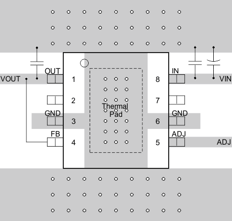
TPS7B4254-Q1 Layout_SLVSDI1.gif Figure 30. TPS7B4254-Q1 Layout Example